参数资料
| 型号: | BU3076HFV-TR |
| 厂商: | Rohm Semiconductor |
| 文件页数: | 10/22页 |
| 文件大小: | 0K |
| 描述: | IC CLOCK GEN 1CH HVSOF6 |
| 标准包装: | 3,000 |
| 类型: | 时钟/频率发生器 |
| PLL: | 是 |
| 主要目的: | 数码相机 |
| 输入: | 时钟 |
| 输出: | 时钟 |
| 电路数: | 1 |
| 比率 - 输入:输出: | 1:1 |
| 差分 - 输入:输出: | 无/无 |
| 频率 - 最大: | 67.5MHz |
| 电源电压: | 2.85 V ~ 3.6 V |
| 工作温度: | -5°C ~ 75°C |
| 安装类型: | 表面贴装 |
| 封装/外壳: | 6-SMD |
| 供应商设备封装: | HVSOF6 |
| 包装: | 带卷 (TR) |
18
DS601F2
CS5340
Confidential Draft
3/11/08
4.4
Power-Up Sequence
Reliable power-up can be accomplished by keeping the device in reset until the power supplies, clocks and
configuration pins are stable. It is also recommended that reset be enabled if the analog or digital supplies
drop below the minimum specified operating voltages to prevent power-glitch-related issues.
4.5
Analog Connections
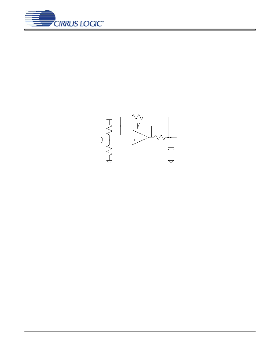
The analog modulator samples the input at half of the MCLK frequency, or nominally 6.144 MHz. The digital
filter will reject signals within the stopband of the filter. However, there is no rejection for input signals which
are multiples of the input sampling frequency (n
× 6.144 MHz), where n=0,1,2,... Refer to Figure 21 which
shows the suggested filter that will attenuate any noise energy at 6.144 MHz, in addition to providing the
optimum source impedance for the modulators. The use of capacitors which have a large voltage coefficient
(such as general purpose ceramics) must be avoided since these can degrade signal linearity.
4.6
Grounding and Power Supply Decoupling
As with any high-resolution converter, achieving optimal performance from the CS5340 requires careful at-
tention to power supply and grounding arrangements. Figure 17 shows the recommended power arrange-
ments, with VA and VL connected to clean supplies. VD, which powers the digital filter, may be run from the
system logic supply or may be powered from the analog supply via a resistor. In this case, no additional
devices should be powered from VD. Decoupling capacitors should be as near to the ADC as possible, with
the low-value ceramic capacitor being the nearest. All signals, especially clocks, should be kept away from
the FILT+ and VQ pins in order to avoid unwanted coupling into the modulators. The FILT+ and VQ decou-
pling capacitors, particularly the 0.01 F, must be positioned to minimize the electrical path from FILT+ and
REF_GND. Furthermore, all ground pins on CS5340 should be referenced to the same ground reference.
The CDB5340 evaluation board demonstrates the optimum layout and power supply arrangements. To min-
imize digital noise, connect the ADC digital outputs only to CMOS inputs.
4.7
Synchronization of Multiple Devices
In systems where multiple ADCs are required, the user can achieve simultaneous sampling if the MCLK and
LRCK signals are the same for all of the CS5340’s in the system. If only one master clock source is needed,
one solution is to place one CS5340 in Master mode, and slave all of the other CS5340’s to the one master.
If multiple master clock sources are needed, a possible solution would be to supply all clocks from the same
external source and time the CS5340 reset with the inactive (falling) edge of MCLK. This will ensure that all
converters begin sampling on the same clock edge.
Figure 21. CS5340 Recommended Analog Input Buffer
100 k
100 k
VA
4.7
F
470 pF
C0G
634
91
2700 pF
CS5340 AINx
AINx
相关PDF资料 |
PDF描述 |
|---|---|
| CA3338AMZ96 | IC DAC 8BIT 50MSPS R-R 16-SOIC |
| CDCR83DBQG4 | IC DIRECT RAMBUS CLK GEN 24-QSOP |
| CDP68HC68T1M | IC RTC 32X8 NVSRAM CMOS 20-SOIC |
| CPLL66-1600-2200 | IC VCO PLL/SYNTH 2.2GHZ SMD |
| CPLL66-2175-2175 | IC VCO PLL/SYNTH 2175MHZ SMD |
相关代理商/技术参数 |
参数描述 |
|---|---|
| BU307F | 制造商:ISC 制造商全称:Inchange Semiconductor Company Limited 功能描述:isc Silicon NPN Power Transistor |
| BU3087FV-E | 制造商:ROHM 制造商全称:Rohm 功能描述:Built in VCXO,Spread-Spectrum Clock Generator |
| BU3087FV-E2 | 制造商:ROHM Semiconductor 功能描述:PLL Clock Generator Single 16-Pin SSOP-B T/R |
| BU-30BL | 功能描述:测试电夹 BRLD MINI-GATOR CLIP RoHS:否 制造商:Pomona Electronics 类型:Minigrabber clip 颜色:Black |
| BU-30C | 功能描述:测试电夹 MIN-GATOR CLIP COP RoHS:否 制造商:Pomona Electronics 类型:Minigrabber clip 颜色:Black |
发布紧急采购,3分钟左右您将得到回复。