- 您现在的位置:买卖IC网 > PDF目录298892 > BX80552360 (INTEL CORP) 32-BIT, 3460 MHz, MICROPROCESSOR, CBGA775 PDF资料下载
参数资料
| 型号: | BX80552360 |
| 厂商: | INTEL CORP |
| 元件分类: | 微控制器/微处理器 |
| 英文描述: | 32-BIT, 3460 MHz, MICROPROCESSOR, CBGA775 |
| 封装: | LGA-775 |
| 文件页数: | 18/96页 |
| 文件大小: | 1975K |
| 代理商: | BX80552360 |
第1页第2页第3页第4页第5页第6页第7页第8页第9页第10页第11页第12页第13页第14页第15页第16页第17页当前第18页第19页第20页第21页第22页第23页第24页第25页第26页第27页第28页第29页第30页第31页第32页第33页第34页第35页第36页第37页第38页第39页第40页第41页第42页第43页第44页第45页第46页第47页第48页第49页第50页第51页第52页第53页第54页第55页第56页第57页第58页第59页第60页第61页第62页第63页第64页第65页第66页第67页第68页第69页第70页第71页第72页第73页第74页第75页第76页第77页第78页第79页第80页第81页第82页第83页第84页第85页第86页第87页第88页第89页第90页第91页第92页第93页第94页第95页第96页
Datasheet
25
Electrical Specifications
2.6.2
GTL+ Asynchronous Signals
Legacy input signals such as A20M#, IGNNE#, INIT#, SMI#, and STPCLK# use CMOS
input buffers. All of these signals follow the same DC requirements as GTL+ signals;
however, the outputs are not actively driven high (during a logical 0 to 1 transition) by
the processor. These signals do not have setup or hold time specifications in relation to
BCLK[1:0].
All of the GTL+ Asynchronous signals are required to be asserted/de-asserted for at
least six BCLKs in order for the processor to recognize the proper signal state. See
Section 2.6.3 for the DC specifications for the GTL+ Asynchronous signal groups. See
Section 6.2 for additional timing requirements for entering and leaving the low power
states.
2.6.3
Processor DC Specifications
The processor DC specifications in this section are defined at the processor core (pads)
unless otherwise stated. All specifications apply to all frequencies and cache sizes
unless otherwise stated.
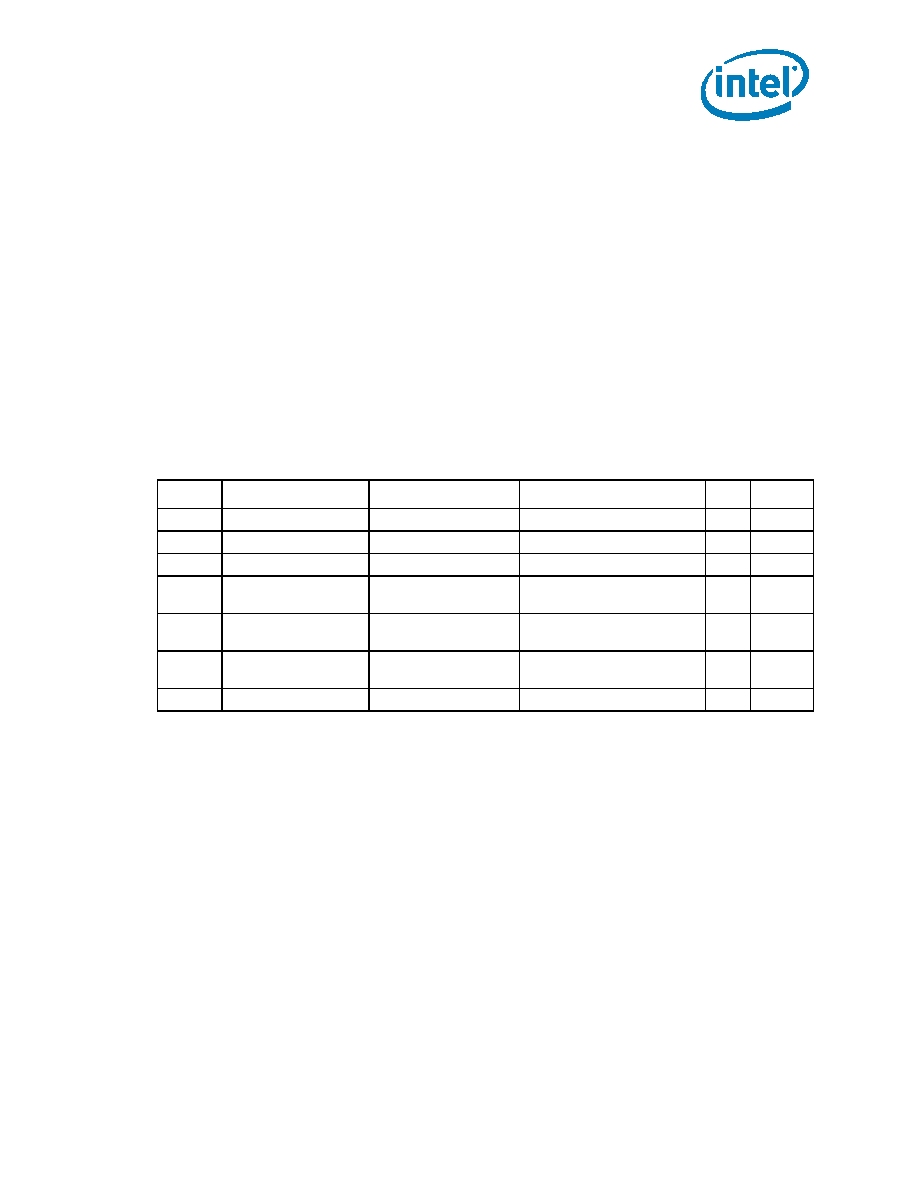
Table 10.
GTL+ Signal Group DC Specifications
Symbol
Parameter
Min
Max
Unit
Notes1
NOTES:
1. Unless otherwise noted, all specifications in this table apply to all processor frequencies.
VIL
Input Low Voltage
0.0
GTLREF – (0.10 * VTT)V
2, 3
2. VIL is defined as the voltage range at a receiving agent that will be interpreted as a logical low value.
3. The VTT referred to in these specifications is the instantaneous VTT.
VIH
Input High Voltage
GTLREF + (0.10 * VTT)VTT
V
4, 5, 3
4. VIH is defined as the voltage range at a receiving agent that will be interpreted as a logical high value.
5. VIH and VOH may experience excursions above VTT. However, input signal drivers must comply with the
signal quality specifications.
VOH
Output High Voltage
0.90*VTT
VTT
V
3, 5
IOL
Output Low Current
N/A
VTT_MAX/
[(0.50*RTT_MIN)+(RON_MIN)]
A-
ILI
Input Leakage
Current
N/A
± 200
A
6
6. Leakage to VSS with land held at VTT.
ILO
Output Leakage
Current
N/A
± 200
A
7
7. Leakage to VTT with land held at 300 mV.
RON
Buffer On Resistance
6
12
Ω
相关PDF资料 |
PDF描述 |
|---|---|
| BX80552651 | 32-BIT, 3400 MHz, MICROPROCESSOR, PBGA775 |
| BX80552651T | 32-BIT, 3400 MHz, MICROPROCESSOR, PBGA775 |
| BX80552661 | 32-BIT, 3600 MHz, MICROPROCESSOR, PBGA775 |
| BX80552651T2 | 32-BIT, 3400 MHz, MICROPROCESSOR, PBGA775 |
| BX80552641T | 32-BIT, 3200 MHz, MICROPROCESSOR, PBGA775 |
相关代理商/技术参数 |
参数描述 |
|---|---|
| BX80552360 S L9KK | 制造商:Intel 功能描述:MPU CELERON 65NM 3.46GHZ 775PIN FCLGA4 - Boxed Product (Development Kits) |
| BX80552631 | 制造商:Intel 功能描述:Pentium4 Processor 630 3.0GHz with fan |
| BX80552631 S L9KG | 制造商:Intel 功能描述: |
| BX80552641T2 | 制造商:Intel 功能描述:P4 641 3.2GHZ LP-BTX 2MB - Boxed Product (Development Kits) |
| BX80552651T2 | 制造商:Intel 功能描述:P4 651 3.4GHZ LP-BTX 2MB - Boxed Product (Development Kits) |
发布紧急采购,3分钟左右您将得到回复。