参数资料
| 型号: | C8051F226R |
| 厂商: | Silicon Laboratories Inc |
| 文件页数: | 49/146页 |
| 文件大小: | 0K |
| 描述: | IC 8051 MCU 8K FLASH 48TQFP |
| 标准包装: | 1 |
| 系列: | C8051F2xx |
| 核心处理器: | 8051 |
| 芯体尺寸: | 8-位 |
| 速度: | 25MHz |
| 连通性: | SPI,UART/USART |
| 外围设备: | 欠压检测/复位,POR,WDT |
| 输入/输出数: | 32 |
| 程序存储器容量: | 8KB(8K x 8) |
| 程序存储器类型: | 闪存 |
| RAM 容量: | 1.25K x 8 |
| 电压 - 电源 (Vcc/Vdd): | 2.7 V ~ 3.6 V |
| 数据转换器: | A/D 32x8b |
| 振荡器型: | 内部 |
| 工作温度: | -40°C ~ 85°C |
| 封装/外壳: | 48-TQFP |
| 包装: | 剪切带 (CT) |
| 其它名称: | 336-1010-1 |
第1页第2页第3页第4页第5页第6页第7页第8页第9页第10页第11页第12页第13页第14页第15页第16页第17页第18页第19页第20页第21页第22页第23页第24页第25页第26页第27页第28页第29页第30页第31页第32页第33页第34页第35页第36页第37页第38页第39页第40页第41页第42页第43页第44页第45页第46页第47页第48页当前第49页第50页第51页第52页第53页第54页第55页第56页第57页第58页第59页第60页第61页第62页第63页第64页第65页第66页第67页第68页第69页第70页第71页第72页第73页第74页第75页第76页第77页第78页第79页第80页第81页第82页第83页第84页第85页第86页第87页第88页第89页第90页第91页第92页第93页第94页第95页第96页第97页第98页第99页第100页第101页第102页第103页第104页第105页第106页第107页第108页第109页第110页第111页第112页第113页第114页第115页第116页第117页第118页第119页第120页第121页第122页第123页第124页第125页第126页第127页第128页第129页第130页第131页第132页第133页第134页第135页第136页第137页第138页第139页第140页第141页第142页第143页第144页第145页第146页
C8051F2xx
142
Rev. 1.6
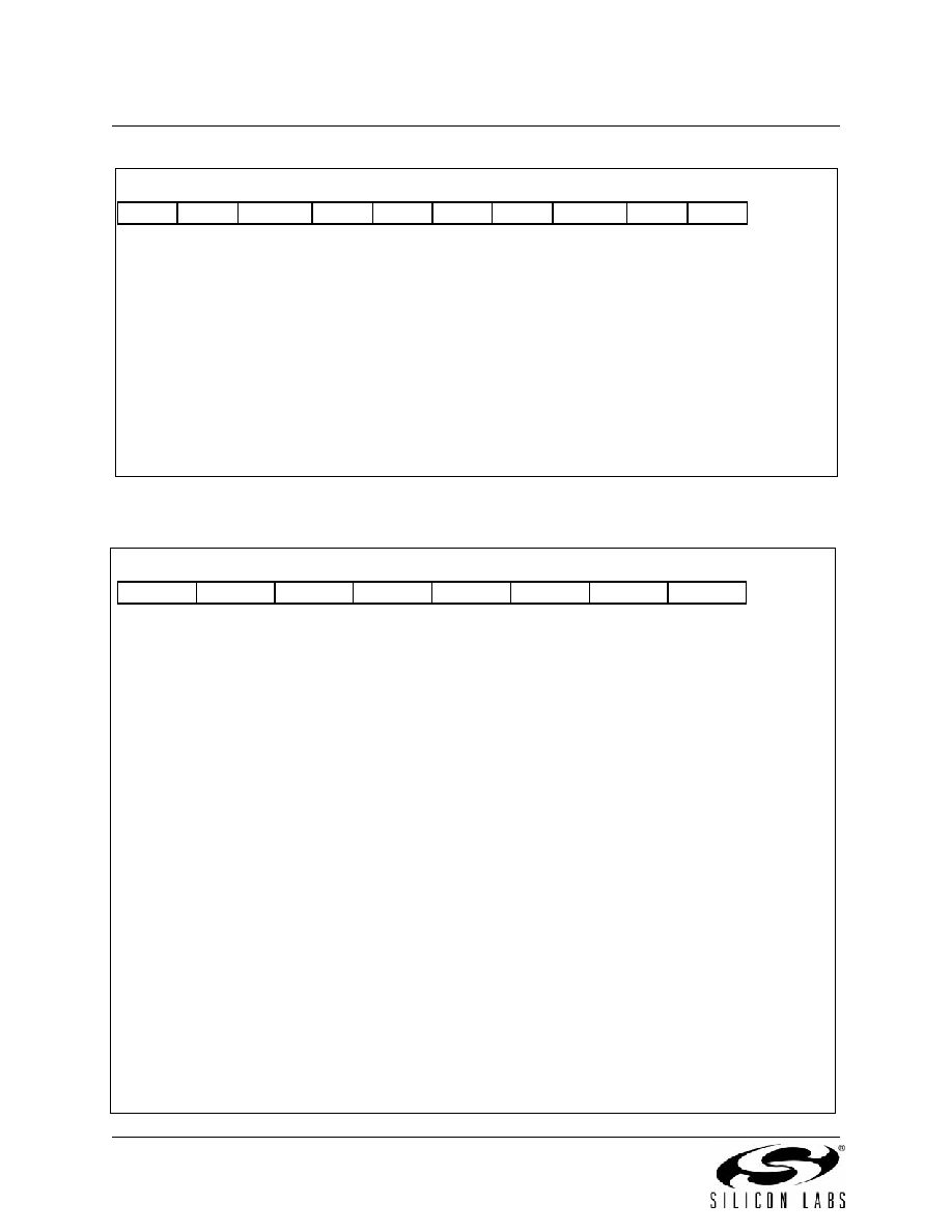
JTAG Register Definition 18.4. FLASHDAT: JTAG Flash Data
This register is used to read or write data to the Flash memory across the JTAG interface.
Bits9–2: DATA7–0: Flash Data Byte.
Bit1:
FAIL: Flash Fail Bit.
0:
Previous Flash memory operation was successful.
1:
Previous Flash memory operation failed. Usually indicates the associated memory
location was locked.
Bit0:
BUSY: Flash Busy Bit.
0:
Flash interface logic is not busy.
1:
Flash interface logic is processing a request. Reads or writes while BUSY = 1 will
not initiate another operation
JTAG Register Definition 18.5. FLASHSCL: JTAG Flash Scale
This register controls the Flash read timing circuit and the prescaler required to generate the correct
timing for Flash operations.
Bit7:
FOSE: Flash One-Shot Enable Bit.
0: Flash read strobe is a full clock-cycle wide.
1: Flash read strobe is 50nsec.
Bit6:
FRAE: Flash Read Always Bit.
0: The Flash output enable and sense amplifier enable are on only when needed to read the
Flash memory.
1: The Flash output enable and sense amplifier enable are always on. This can be used to
limit the variations in digital supply current due to switching the sense amplifiers, thereby
reducing digitally induced noise.
Bits5–4: UNUSED. Read = 00b, Write = don't care.
Bits3–0: FLSCL3–0: Flash Prescaler Control Bits.
The FLSCL3–0 bits control the prescaler used to generate timing signals for Flash opera-
tions. Its value should be written before any Flash write or erase operations are initiated.
The value written should be the smallest integer for which:
FLSCL[3:0] > log2(fSYSCLK / 50kHz)
Where fSYSCLK is the system clock frequency. All Flash read/write/erase operations are
disallowed when FLSCL[3:0] = 1111b.
Reset Value
DATA7 DATA6
DATA5
DATA4 DATA3 DATA2 DATA1
DATA0
FAIL
BUSY
0000000000
Bit9
Bit8
Bit7
Bit6
Bit5
Bit4
Bit3
Bit2
Bit1
Bit0
Reset Value
FOSE
FRAE
-
FLSCL3
FLSCL2
FLSCL1
FLSCL0
00000000
Bit7
Bit6
Bit5
Bit4
Bit3
Bit2
Bit1
Bit0
相关PDF资料 |
PDF描述 |
|---|---|
| C8051F002R | IC 8051 MCU 32K FLASH 32LQFP |
| PIC18F442-I/P | IC MCU FLASH 8KX16 EE A/D 40DIP |
| PIC32MX340F256H-80I/PT | IC PIC MCU FLASH 256K 64-TQFP |
| PIC16LF874A-I/PT | IC PIC MCU FLASH 4KX14 44TQFP |
| PIC24HJ128GP510-I/PT | IC PIC MCU FLASH 128KB 100TQFP |
相关代理商/技术参数 |
参数描述 |
|---|---|
| C8051F226-TB | 功能描述:插座和适配器 With C8051F226 MCU RoHS:否 制造商:Silicon Labs 产品:Adapter 用于:EM35x |
| C8051F23 | 制造商:未知厂家 制造商全称:未知厂家 功能描述:8K Flash, 256 RAM, 48-Pin MCU |
| C8051F230 | 功能描述:8位微控制器 -MCU 8KB RoHS:否 制造商:Silicon Labs 核心:8051 处理器系列:C8051F39x 数据总线宽度:8 bit 最大时钟频率:50 MHz 程序存储器大小:16 KB 数据 RAM 大小:1 KB 片上 ADC:Yes 工作电源电压:1.8 V to 3.6 V 工作温度范围:- 40 C to + 105 C 封装 / 箱体:QFN-20 安装风格:SMD/SMT |
| C8051F230-GQ | 功能描述:8位微控制器 -MCU 8KB 48P MCU RoHS:否 制造商:Silicon Labs 核心:8051 处理器系列:C8051F39x 数据总线宽度:8 bit 最大时钟频率:50 MHz 程序存储器大小:16 KB 数据 RAM 大小:1 KB 片上 ADC:Yes 工作电源电压:1.8 V to 3.6 V 工作温度范围:- 40 C to + 105 C 封装 / 箱体:QFN-20 安装风格:SMD/SMT |
| C8051F230-GQR | 功能描述:8位微控制器 -MCU 8KB 48Pin MCU Tape and Reel RoHS:否 制造商:Silicon Labs 核心:8051 处理器系列:C8051F39x 数据总线宽度:8 bit 最大时钟频率:50 MHz 程序存储器大小:16 KB 数据 RAM 大小:1 KB 片上 ADC:Yes 工作电源电压:1.8 V to 3.6 V 工作温度范围:- 40 C to + 105 C 封装 / 箱体:QFN-20 安装风格:SMD/SMT |
发布紧急采购,3分钟左右您将得到回复。