- 您现在的位置:买卖IC网 > PDF目录11153 > C8051F230-GQR (Silicon Laboratories Inc)IC 8051 MCU 8K FLASH 48TQFP PDF资料下载
参数资料
| 型号: | C8051F230-GQR |
| 厂商: | Silicon Laboratories Inc |
| 文件页数: | 133/146页 |
| 文件大小: | 0K |
| 描述: | IC 8051 MCU 8K FLASH 48TQFP |
| 产品培训模块: | Serial Communication Overview |
| 标准包装: | 500 |
| 系列: | C8051F2xx |
| 核心处理器: | 8051 |
| 芯体尺寸: | 8-位 |
| 速度: | 25MHz |
| 连通性: | SPI,UART/USART |
| 外围设备: | 欠压检测/复位,POR,WDT |
| 输入/输出数: | 32 |
| 程序存储器容量: | 8KB(8K x 8) |
| 程序存储器类型: | 闪存 |
| RAM 容量: | 256 x 8 |
| 电压 - 电源 (Vcc/Vdd): | 2.7 V ~ 3.6 V |
| 振荡器型: | 内部 |
| 工作温度: | -40°C ~ 85°C |
| 封装/外壳: | 48-TQFP |
| 包装: | 带卷 (TR) |
第1页第2页第3页第4页第5页第6页第7页第8页第9页第10页第11页第12页第13页第14页第15页第16页第17页第18页第19页第20页第21页第22页第23页第24页第25页第26页第27页第28页第29页第30页第31页第32页第33页第34页第35页第36页第37页第38页第39页第40页第41页第42页第43页第44页第45页第46页第47页第48页第49页第50页第51页第52页第53页第54页第55页第56页第57页第58页第59页第60页第61页第62页第63页第64页第65页第66页第67页第68页第69页第70页第71页第72页第73页第74页第75页第76页第77页第78页第79页第80页第81页第82页第83页第84页第85页第86页第87页第88页第89页第90页第91页第92页第93页第94页第95页第96页第97页第98页第99页第100页第101页第102页第103页第104页第105页第106页第107页第108页第109页第110页第111页第112页第113页第114页第115页第116页第117页第118页第119页第120页第121页第122页第123页第124页第125页第126页第127页第128页第129页第130页第131页第132页当前第133页第134页第135页第136页第137页第138页第139页第140页第141页第142页第143页第144页第145页第146页
C8051F2xx
Rev. 1.6
87
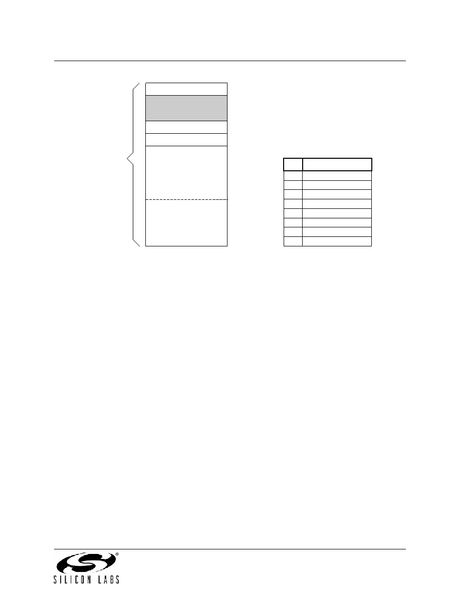
Figure 10.1. Flash Program Memory Security Bytes
The lock bits can always be read and cleared to logic 0 regardless of the security setting applied to the
block containing the security bytes. This allows additional blocks to be protected after the block containing
the security bytes has been locked. However, the only means of removing a lock once set is to erase the
entire program memory space by performing a JTAG erase operation. NOTE: Erasing the Flash memory
block containing the security bytes will automatically initiate erasure of the entire program memory space
(except for the reserved area). This erasure can only be performed via the JTAG. If a non-security byte in
the 0x1C00–0x1DFF page is written to in order to perform an erasure of that page, then that page including
the security bytes will be erased.
Flash Read Lock Byte
Bits7–0: Each bit locks a corresponding block of memory. (Bit 7 is MSB.)
0: Read operations are locked (disabled) for corresponding block across the JTAG inter-
face.
1: Read operations are unlocked (enabled) for corresponding block across the JTAG inter-
face.
Flash Write/Erase Lock Byte
Bits7–0: Each bit locks a corresponding block of memory.
0: Write/Erase operations are locked (disabled) for corresponding block across the JTAG
interface.
1: Write/Erase operations are unlocked (enabled) for corresponding block across the
JTAG interface.
Flash Access Limit Register (FLACL)
The content of this register is used as the high byte of the 16-bit software read limit
address. The 16-bit read limit address value is calculated as 0xNN00 where NN is
replaced by content of this register on reset. Software running at or above this address is
prohibited from using the MOVX and MOVC instructions to read, write, or erase, locations
below this address. Any attempts to read locations below this limit will return the value
0x00.
0x1E00
0x207F
0x2000
0x1DF
E
Program Memory
Space
0x0000
0x1DFF
Read Lock Byte
Write/Erase Lock Byte
Software Read Limit
Reserved
Bit
Memory Block
7
6
5
4
0x1800 - 0x1BFF
0x1C00 - 0x1DFD
0x1400 - 0x17FF
0x1000 - 0x13FF
3
2
1
0
0x0800 - 0x0BFF
0x0C00 - 0x0FFF
0x0400 - 0x07FF
0x0000 - 0x03FF
0x1FFF
Read and Write/Erase Security Bits.
(Bit 7 is MSB.)
(This Block locked only if all
other blocks are locked)
0x1DFD
相关PDF资料 |
PDF描述 |
|---|---|
| VI-B6J-IW-F4 | CONVERTER MOD DC/DC 36V 100W |
| DG212CSE+T | IC SWITCH QUAD SPST 16SOIC |
| VI-B6J-IW-F3 | CONVERTER MOD DC/DC 36V 100W |
| VI-B6J-IW-F2 | CONVERTER MOD DC/DC 36V 100W |
| VI-B6B-IX-F3 | CONVERTER MOD DC/DC 95V 75W |
相关代理商/技术参数 |
参数描述 |
|---|---|
| C8051F230R | 功能描述:8位微控制器 -MCU T-0 48 Pin RoHS:否 制造商:Silicon Labs 核心:8051 处理器系列:C8051F39x 数据总线宽度:8 bit 最大时钟频率:50 MHz 程序存储器大小:16 KB 数据 RAM 大小:1 KB 片上 ADC:Yes 工作电源电压:1.8 V to 3.6 V 工作温度范围:- 40 C to + 105 C 封装 / 箱体:QFN-20 安装风格:SMD/SMT |
| C8051F231 | 功能描述:8位微控制器 -MCU 8KB RoHS:否 制造商:Silicon Labs 核心:8051 处理器系列:C8051F39x 数据总线宽度:8 bit 最大时钟频率:50 MHz 程序存储器大小:16 KB 数据 RAM 大小:1 KB 片上 ADC:Yes 工作电源电压:1.8 V to 3.6 V 工作温度范围:- 40 C to + 105 C 封装 / 箱体:QFN-20 安装风格:SMD/SMT |
| C8051F231-GQ | 功能描述:8位微控制器 -MCU 8KB 32P MCU RoHS:否 制造商:Silicon Labs 核心:8051 处理器系列:C8051F39x 数据总线宽度:8 bit 最大时钟频率:50 MHz 程序存储器大小:16 KB 数据 RAM 大小:1 KB 片上 ADC:Yes 工作电源电压:1.8 V to 3.6 V 工作温度范围:- 40 C to + 105 C 封装 / 箱体:QFN-20 安装风格:SMD/SMT |
| C8051F231-GQR | 功能描述:8位微控制器 -MCU 8KB 32Pin MCU Tape and Reel RoHS:否 制造商:Silicon Labs 核心:8051 处理器系列:C8051F39x 数据总线宽度:8 bit 最大时钟频率:50 MHz 程序存储器大小:16 KB 数据 RAM 大小:1 KB 片上 ADC:Yes 工作电源电压:1.8 V to 3.6 V 工作温度范围:- 40 C to + 105 C 封装 / 箱体:QFN-20 安装风格:SMD/SMT |
| C8051F231R | 功能描述:8位微控制器 -MCU T-0 32 Pin RoHS:否 制造商:Silicon Labs 核心:8051 处理器系列:C8051F39x 数据总线宽度:8 bit 最大时钟频率:50 MHz 程序存储器大小:16 KB 数据 RAM 大小:1 KB 片上 ADC:Yes 工作电源电压:1.8 V to 3.6 V 工作温度范围:- 40 C to + 105 C 封装 / 箱体:QFN-20 安装风格:SMD/SMT |
发布紧急采购,3分钟左右您将得到回复。