- 您现在的位置:买卖IC网 > PDF目录11153 > C8051F230-GQR (Silicon Laboratories Inc)IC 8051 MCU 8K FLASH 48TQFP PDF资料下载
参数资料
| 型号: | C8051F230-GQR |
| 厂商: | Silicon Laboratories Inc |
| 文件页数: | 83/146页 |
| 文件大小: | 0K |
| 描述: | IC 8051 MCU 8K FLASH 48TQFP |
| 产品培训模块: | Serial Communication Overview |
| 标准包装: | 500 |
| 系列: | C8051F2xx |
| 核心处理器: | 8051 |
| 芯体尺寸: | 8-位 |
| 速度: | 25MHz |
| 连通性: | SPI,UART/USART |
| 外围设备: | 欠压检测/复位,POR,WDT |
| 输入/输出数: | 32 |
| 程序存储器容量: | 8KB(8K x 8) |
| 程序存储器类型: | 闪存 |
| RAM 容量: | 256 x 8 |
| 电压 - 电源 (Vcc/Vdd): | 2.7 V ~ 3.6 V |
| 振荡器型: | 内部 |
| 工作温度: | -40°C ~ 85°C |
| 封装/外壳: | 48-TQFP |
| 包装: | 带卷 (TR) |
第1页第2页第3页第4页第5页第6页第7页第8页第9页第10页第11页第12页第13页第14页第15页第16页第17页第18页第19页第20页第21页第22页第23页第24页第25页第26页第27页第28页第29页第30页第31页第32页第33页第34页第35页第36页第37页第38页第39页第40页第41页第42页第43页第44页第45页第46页第47页第48页第49页第50页第51页第52页第53页第54页第55页第56页第57页第58页第59页第60页第61页第62页第63页第64页第65页第66页第67页第68页第69页第70页第71页第72页第73页第74页第75页第76页第77页第78页第79页第80页第81页第82页当前第83页第84页第85页第86页第87页第88页第89页第90页第91页第92页第93页第94页第95页第96页第97页第98页第99页第100页第101页第102页第103页第104页第105页第106页第107页第108页第109页第110页第111页第112页第113页第114页第115页第116页第117页第118页第119页第120页第121页第122页第123页第124页第125页第126页第127页第128页第129页第130页第131页第132页第133页第134页第135页第136页第137页第138页第139页第140页第141页第142页第143页第144页第145页第146页
C8051F2xx
Rev. 1.6
41
6.2.
ADC Modes of Operation
The ADC has a maximum conversion speed of 100 ksps. The ADC conversion clock is derived from the
system clock. The ADC conversion clock is derived from a divided version of SYSCLK. Divide ratios of 1,
2, 4, 8, or 16 are supported by setting the ADCSC bits in the ADC0CF Register. This is useful to adjust
conversion speed to accommodate different system clock speeds.
A conversion can be initiated in one of two ways, depending on the programmed states of the ADC Start of
Conversion Mode bits (ADSTM1, ADSTM0) in ADC0CN. Conversions may be initiated by:
1.
Writing a 1 to the ADBUSY bit of ADC0CN;
2.
A Timer 2 overflow (i.e. timed continuous conversions).
Writing a 1 to ADBUSY provides software control of the ADC whereby conversions are performed "on-
demand". During conversion, the ADBUSY bit is set to 1 and restored to 0 when conversion is complete.
The falling edge of ADBUSY triggers an interrupt (when enabled) and sets the ADCINT interrupt flag in the
ADC0CN register. Note: When conversions are performed "on-demand", the ADCINT flag, not ADBUSY,
should be polled to determine when the conversion has completed. Converted data is available in the ADC
data word register, ADC0H.
The ADCTM bit in register ADC0CN controls the ADC track-and-hold mode. In its default state, the ADC
input is continuously tracked, except when a conversion is in progress. Setting ADCTM to 1 allows one of
two different low power track-and-hold modes to be specified by states of the ADSTM1-0 bits (also in
ADC0CN):
1.
Tracking begins with a write of 1 to ADBUSY and lasts for 3 SAR clocks;
2.
Tracking starts with an overflow of Timer 2 and lasts for 3 SAR clocks.
Tracking can be disabled (shutdown) when the entire chip is in low power standby or sleep modes.
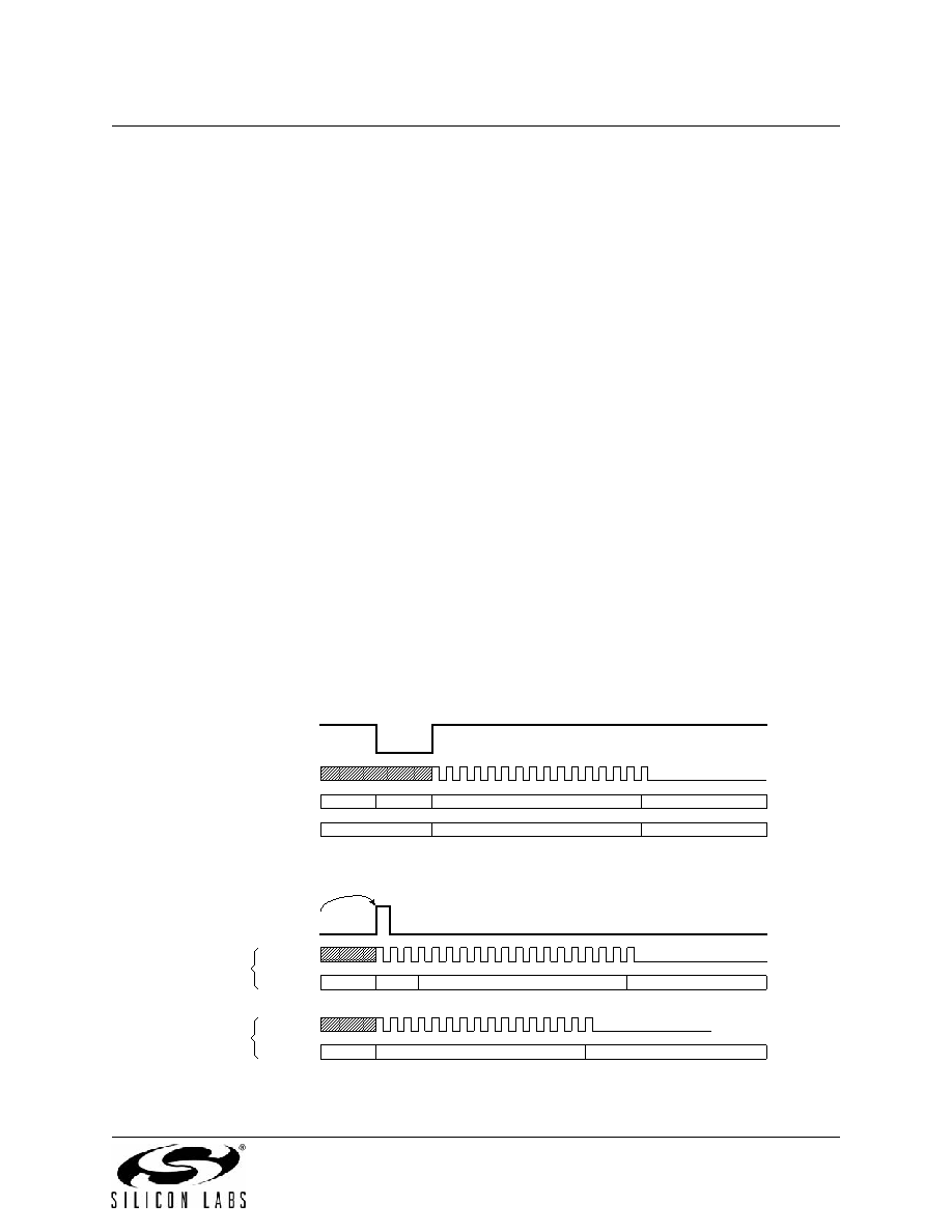
Figure 6.2. 12-Bit ADC Track and Conversion Example Timing
12
345
678
9
10 11 12 13 14 15 16
CNVSTR
(ADSTM[1:0]=10)
ADCTM=1
Track
Convert
Low Power Mode
ADCTM=0
Track Or Convert
Convert
Track
Low Power or
Convert
Timer2, Timer3 Overflow;
Write 1 to ADBUSY
(ADSTM[1:0]=00, 01, 11)
ADCTM=1
Track
Convert
Low Power Mode
ADCTM=0
Track or Convert
Convert
Track
Low Power or
Convert
A. ADC Timing for External Trigger Source
B. ADC Timing for Internal Trigger Sources
SAR Clocks
12
3456
789
10 11 12 13 14 15 16 17 18 19
12
3456
789
10 11 12 13 14 15 16
SAR Clocks
相关PDF资料 |
PDF描述 |
|---|---|
| VI-B6J-IW-F4 | CONVERTER MOD DC/DC 36V 100W |
| DG212CSE+T | IC SWITCH QUAD SPST 16SOIC |
| VI-B6J-IW-F3 | CONVERTER MOD DC/DC 36V 100W |
| VI-B6J-IW-F2 | CONVERTER MOD DC/DC 36V 100W |
| VI-B6B-IX-F3 | CONVERTER MOD DC/DC 95V 75W |
相关代理商/技术参数 |
参数描述 |
|---|---|
| C8051F230R | 功能描述:8位微控制器 -MCU T-0 48 Pin RoHS:否 制造商:Silicon Labs 核心:8051 处理器系列:C8051F39x 数据总线宽度:8 bit 最大时钟频率:50 MHz 程序存储器大小:16 KB 数据 RAM 大小:1 KB 片上 ADC:Yes 工作电源电压:1.8 V to 3.6 V 工作温度范围:- 40 C to + 105 C 封装 / 箱体:QFN-20 安装风格:SMD/SMT |
| C8051F231 | 功能描述:8位微控制器 -MCU 8KB RoHS:否 制造商:Silicon Labs 核心:8051 处理器系列:C8051F39x 数据总线宽度:8 bit 最大时钟频率:50 MHz 程序存储器大小:16 KB 数据 RAM 大小:1 KB 片上 ADC:Yes 工作电源电压:1.8 V to 3.6 V 工作温度范围:- 40 C to + 105 C 封装 / 箱体:QFN-20 安装风格:SMD/SMT |
| C8051F231-GQ | 功能描述:8位微控制器 -MCU 8KB 32P MCU RoHS:否 制造商:Silicon Labs 核心:8051 处理器系列:C8051F39x 数据总线宽度:8 bit 最大时钟频率:50 MHz 程序存储器大小:16 KB 数据 RAM 大小:1 KB 片上 ADC:Yes 工作电源电压:1.8 V to 3.6 V 工作温度范围:- 40 C to + 105 C 封装 / 箱体:QFN-20 安装风格:SMD/SMT |
| C8051F231-GQR | 功能描述:8位微控制器 -MCU 8KB 32Pin MCU Tape and Reel RoHS:否 制造商:Silicon Labs 核心:8051 处理器系列:C8051F39x 数据总线宽度:8 bit 最大时钟频率:50 MHz 程序存储器大小:16 KB 数据 RAM 大小:1 KB 片上 ADC:Yes 工作电源电压:1.8 V to 3.6 V 工作温度范围:- 40 C to + 105 C 封装 / 箱体:QFN-20 安装风格:SMD/SMT |
| C8051F231R | 功能描述:8位微控制器 -MCU T-0 32 Pin RoHS:否 制造商:Silicon Labs 核心:8051 处理器系列:C8051F39x 数据总线宽度:8 bit 最大时钟频率:50 MHz 程序存储器大小:16 KB 数据 RAM 大小:1 KB 片上 ADC:Yes 工作电源电压:1.8 V to 3.6 V 工作温度范围:- 40 C to + 105 C 封装 / 箱体:QFN-20 安装风格:SMD/SMT |
发布紧急采购,3分钟左右您将得到回复。