- 您现在的位置:买卖IC网 > PDF目录11153 > C8051F230-GQR (Silicon Laboratories Inc)IC 8051 MCU 8K FLASH 48TQFP PDF资料下载
参数资料
| 型号: | C8051F230-GQR |
| 厂商: | Silicon Laboratories Inc |
| 文件页数: | 82/146页 |
| 文件大小: | 0K |
| 描述: | IC 8051 MCU 8K FLASH 48TQFP |
| 产品培训模块: | Serial Communication Overview |
| 标准包装: | 500 |
| 系列: | C8051F2xx |
| 核心处理器: | 8051 |
| 芯体尺寸: | 8-位 |
| 速度: | 25MHz |
| 连通性: | SPI,UART/USART |
| 外围设备: | 欠压检测/复位,POR,WDT |
| 输入/输出数: | 32 |
| 程序存储器容量: | 8KB(8K x 8) |
| 程序存储器类型: | 闪存 |
| RAM 容量: | 256 x 8 |
| 电压 - 电源 (Vcc/Vdd): | 2.7 V ~ 3.6 V |
| 振荡器型: | 内部 |
| 工作温度: | -40°C ~ 85°C |
| 封装/外壳: | 48-TQFP |
| 包装: | 带卷 (TR) |
第1页第2页第3页第4页第5页第6页第7页第8页第9页第10页第11页第12页第13页第14页第15页第16页第17页第18页第19页第20页第21页第22页第23页第24页第25页第26页第27页第28页第29页第30页第31页第32页第33页第34页第35页第36页第37页第38页第39页第40页第41页第42页第43页第44页第45页第46页第47页第48页第49页第50页第51页第52页第53页第54页第55页第56页第57页第58页第59页第60页第61页第62页第63页第64页第65页第66页第67页第68页第69页第70页第71页第72页第73页第74页第75页第76页第77页第78页第79页第80页第81页当前第82页第83页第84页第85页第86页第87页第88页第89页第90页第91页第92页第93页第94页第95页第96页第97页第98页第99页第100页第101页第102页第103页第104页第105页第106页第107页第108页第109页第110页第111页第112页第113页第114页第115页第116页第117页第118页第119页第120页第121页第122页第123页第124页第125页第126页第127页第128页第129页第130页第131页第132页第133页第134页第135页第136页第137页第138页第139页第140页第141页第142页第143页第144页第145页第146页
C8051F2xx
40
Rev. 1.6
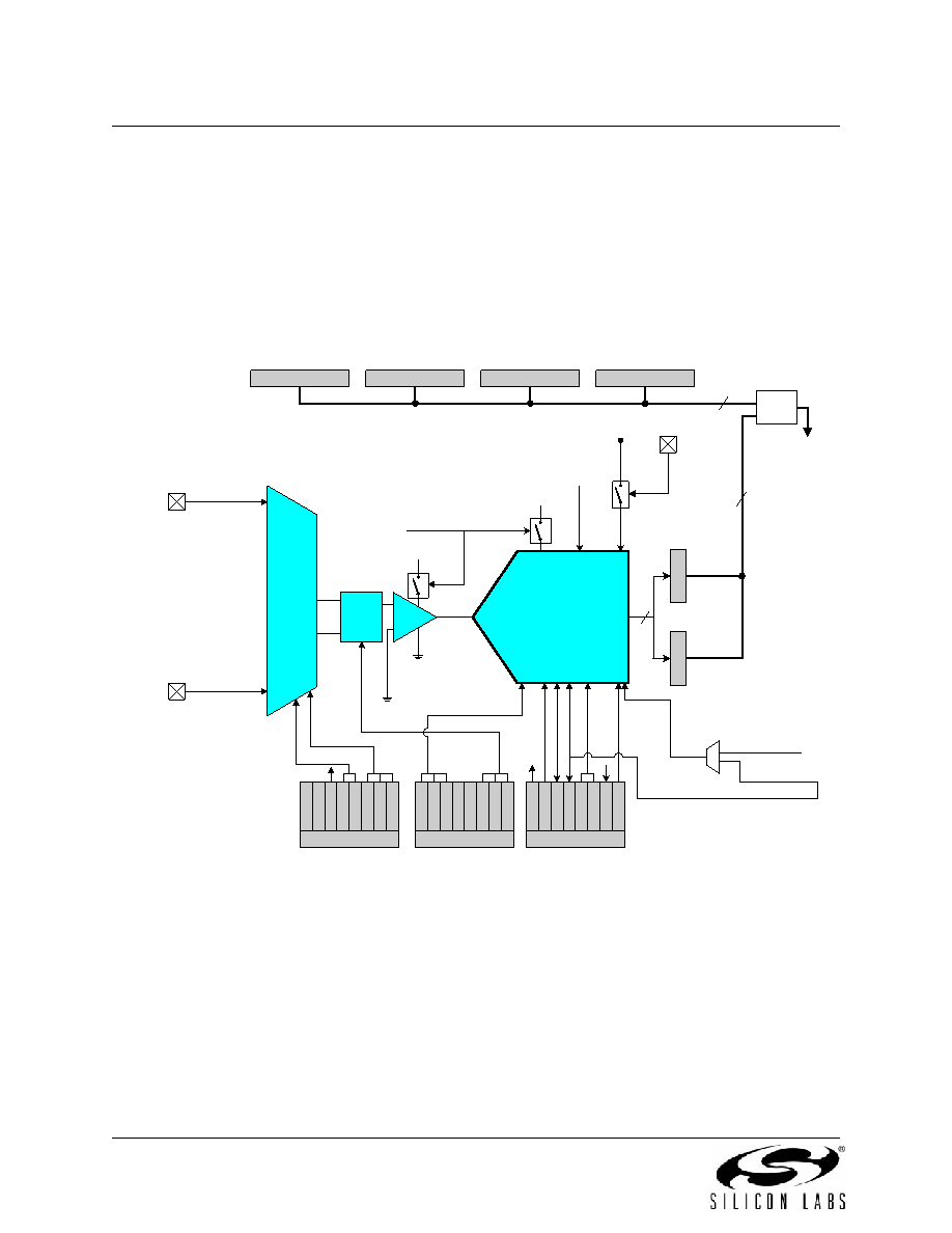
6.
ADC (12-Bit, C8051F206 Only)
Description
The ADC subsystem for the C8051F206 consists of configurable analog multiplexer (AMUX), a program-
mable gain amplifier (PGA), and a 100ksps, 12-bit successive-approximation-register ADC with integrated
track-and-hold and programmable window detector (see Figure 6.1). The AMUX, PGA, Data Conversion
Modes, and Window Detector are all configurable under software control via the Special Function Regis-
ter's shown in Figure 6.1. The ADC subsystem (ADC, track-and-hold and PGA) is enabled only when the
ADCEN bit in the ADC Control register (ADC0CN, Figure 6.5) is set to 1. The ADC subsystem is in low
power shutdown when this bit is 0.
Figure 6.1. 12-Bit ADC Functional Block Diagram
6.1.
Analog Multiplexer and PGA
Any external port pin (ports 0-3) may be selected via software. The AMX0SL SFR is used to select the
desired analog input pin. (See SFR Definition 5.1). When the AMUX is enabled, the user selects which
port is to be used (bits PRTSL0–1), and then the pin in the selected port (bits PINSL0–2) to be the analog
input.
The PGA amplifies the AMUX output signal by an amount determined by the states of the AMPGN2–0 bits
in the ADC Configuration register, ADC0CF (SFR Definition 5.2). The PGA can be software-programmed
for gains of 0.5, 1, 2, 4, 8 or 16. It defaults to a gain of 1 on reset.
12-Bit
SAR
ADC
RE
F
+
-
VDD
12
32-to-1
AMUX
VDD
ADCEN
S
YSC
L
K
X
AIN0
AIN31
ADBUSY(w)
C
onve
rsi
on
S
tar
t
AMX0SL
PI
N
S
L
0
PI
N
S
L
1
PI
N
S
L
2
PR
TSL
0
ADC0CF
AM
PGN
0
AM
PGN
1
AM
PGN
2
A
DCS
C
0
A
DCS
C
1
A
DCS
C
2
ADC0CN
ADLJ
ST
ADW
INT
AD
STM
0
AD
STM
1
AD
BUS
Y
ADC
INT
A
DCT
M
ADC
EN
A
DC0
H
AM
X
EN
PR
TSL
1
VDD
VREF
GND
T2 OV
..
.
ADC0LTL
ADC0LTH
24
12
ADWINT
AIN0-31 are port 0-3
pins -- any external
port pin may be configured
as an analog input
GND
AD
C0
L
ADC0GTL
ADC0GTH
Dig
Comp
相关PDF资料 |
PDF描述 |
|---|---|
| VI-B6J-IW-F4 | CONVERTER MOD DC/DC 36V 100W |
| DG212CSE+T | IC SWITCH QUAD SPST 16SOIC |
| VI-B6J-IW-F3 | CONVERTER MOD DC/DC 36V 100W |
| VI-B6J-IW-F2 | CONVERTER MOD DC/DC 36V 100W |
| VI-B6B-IX-F3 | CONVERTER MOD DC/DC 95V 75W |
相关代理商/技术参数 |
参数描述 |
|---|---|
| C8051F230R | 功能描述:8位微控制器 -MCU T-0 48 Pin RoHS:否 制造商:Silicon Labs 核心:8051 处理器系列:C8051F39x 数据总线宽度:8 bit 最大时钟频率:50 MHz 程序存储器大小:16 KB 数据 RAM 大小:1 KB 片上 ADC:Yes 工作电源电压:1.8 V to 3.6 V 工作温度范围:- 40 C to + 105 C 封装 / 箱体:QFN-20 安装风格:SMD/SMT |
| C8051F231 | 功能描述:8位微控制器 -MCU 8KB RoHS:否 制造商:Silicon Labs 核心:8051 处理器系列:C8051F39x 数据总线宽度:8 bit 最大时钟频率:50 MHz 程序存储器大小:16 KB 数据 RAM 大小:1 KB 片上 ADC:Yes 工作电源电压:1.8 V to 3.6 V 工作温度范围:- 40 C to + 105 C 封装 / 箱体:QFN-20 安装风格:SMD/SMT |
| C8051F231-GQ | 功能描述:8位微控制器 -MCU 8KB 32P MCU RoHS:否 制造商:Silicon Labs 核心:8051 处理器系列:C8051F39x 数据总线宽度:8 bit 最大时钟频率:50 MHz 程序存储器大小:16 KB 数据 RAM 大小:1 KB 片上 ADC:Yes 工作电源电压:1.8 V to 3.6 V 工作温度范围:- 40 C to + 105 C 封装 / 箱体:QFN-20 安装风格:SMD/SMT |
| C8051F231-GQR | 功能描述:8位微控制器 -MCU 8KB 32Pin MCU Tape and Reel RoHS:否 制造商:Silicon Labs 核心:8051 处理器系列:C8051F39x 数据总线宽度:8 bit 最大时钟频率:50 MHz 程序存储器大小:16 KB 数据 RAM 大小:1 KB 片上 ADC:Yes 工作电源电压:1.8 V to 3.6 V 工作温度范围:- 40 C to + 105 C 封装 / 箱体:QFN-20 安装风格:SMD/SMT |
| C8051F231R | 功能描述:8位微控制器 -MCU T-0 32 Pin RoHS:否 制造商:Silicon Labs 核心:8051 处理器系列:C8051F39x 数据总线宽度:8 bit 最大时钟频率:50 MHz 程序存储器大小:16 KB 数据 RAM 大小:1 KB 片上 ADC:Yes 工作电源电压:1.8 V to 3.6 V 工作温度范围:- 40 C to + 105 C 封装 / 箱体:QFN-20 安装风格:SMD/SMT |
发布紧急采购,3分钟左右您将得到回复。