- 您现在的位置:买卖IC网 > PDF目录3801 > C8051F300-GM (Silicon Laboratories Inc)IC 8051 MCU 8K FLASH 11QFN PDF资料下载
参数资料
| 型号: | C8051F300-GM |
| 厂商: | Silicon Laboratories Inc |
| 文件页数: | 71/178页 |
| 文件大小: | 0K |
| 描述: | IC 8051 MCU 8K FLASH 11QFN |
| 产品培训模块: | Serial Communication Overview |
| 标准包装: | 122 |
| 系列: | C8051F30x |
| 核心处理器: | 8051 |
| 芯体尺寸: | 8-位 |
| 速度: | 25MHz |
| 连通性: | SMBus(2 线/I²C),UART/USART |
| 外围设备: | POR,PWM,温度传感器,WDT |
| 输入/输出数: | 8 |
| 程序存储器容量: | 8KB(8K x 8) |
| 程序存储器类型: | 闪存 |
| RAM 容量: | 256 x 8 |
| 电压 - 电源 (Vcc/Vdd): | 2.7 V ~ 3.6 V |
| 数据转换器: | A/D 8x8b |
| 振荡器型: | 内部 |
| 工作温度: | -40°C ~ 85°C |
| 封装/外壳: | 10-VFDFN 裸露焊盘 |
| 包装: | 管件 |
| 产品目录页面: | 623 (CN2011-ZH PDF) |
| 配用: | 336-1444-ND - ADAPTER PROGRAM TOOLSTICK F300 336-1351-ND - KIT REF DES TEMP COMPENS RTC 336-1348-ND - KIT STARTER TOOLSTICK 336-1283-ND - KIT REF DESIGN DTMF DECODER 336-1278-ND - KIT TOOL EVAL SYS IN A USB STICK 336-1246-ND - DEV KIT F300/301/302/303/304/305 |
| 其它名称: | 336-1245 |
第1页第2页第3页第4页第5页第6页第7页第8页第9页第10页第11页第12页第13页第14页第15页第16页第17页第18页第19页第20页第21页第22页第23页第24页第25页第26页第27页第28页第29页第30页第31页第32页第33页第34页第35页第36页第37页第38页第39页第40页第41页第42页第43页第44页第45页第46页第47页第48页第49页第50页第51页第52页第53页第54页第55页第56页第57页第58页第59页第60页第61页第62页第63页第64页第65页第66页第67页第68页第69页第70页当前第71页第72页第73页第74页第75页第76页第77页第78页第79页第80页第81页第82页第83页第84页第85页第86页第87页第88页第89页第90页第91页第92页第93页第94页第95页第96页第97页第98页第99页第100页第101页第102页第103页第104页第105页第106页第107页第108页第109页第110页第111页第112页第113页第114页第115页第116页第117页第118页第119页第120页第121页第122页第123页第124页第125页第126页第127页第128页第129页第130页第131页第132页第133页第134页第135页第136页第137页第138页第139页第140页第141页第142页第143页第144页第145页第146页第147页第148页第149页第150页第151页第152页第153页第154页第155页第156页第157页第158页第159页第160页第161页第162页第163页第164页第165页第166页第167页第168页第169页第170页第171页第172页第173页第174页第175页第176页第177页第178页
C8051F300/1/2/3/4/5
162
Rev. 2.9
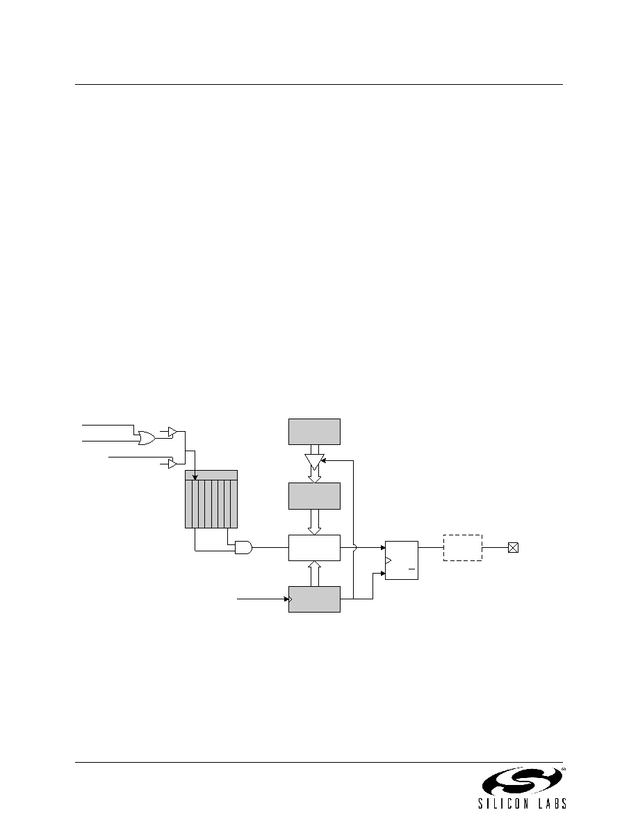
16.2.5. 8-Bit Pulse Width Modulator Mode
Each module can be used independently to generate a pulse width modulated (PWM) output on its associ-
ated CEXn pin. The frequency of the output is dependent on the timebase for the PCA counter/timer. The
duty cycle of the PWM output signal is varied using the module's PCA0CPLn capture/compare register.
When the value in the low byte of the PCA counter/timer (PCA0L) is equal to the value in PCA0CPLn, the
output on the CEXn pin will be set to ‘1’. When the count value in PCA0L overflows, the CEXn output will
be set to ‘0’ (see Figure 16.8). Also, when the counter/timer low byte (PCA0L) overflows from 0xFF to
0x00, PCA0CPLn is reloaded automatically with the value stored in the module’s capture/compare high
byte (PCA0CPHn) without software intervention. Setting the ECOMn and PWMn bits in the PCA0CPMn
register enables 8-bit Pulse Width Modulator mode. The duty cycle for 8-bit PWM Mode is given by
Equation 16.2.
Important Note About Capture/Compare Registers: When writing a 16-bit value to the PCA0 Capture/
Compare registers, the low byte should always be written first. Writing to PCA0CPLn clears the ECOMn bit
to ‘0’; writing to PCA0CPHn sets ECOMn to ‘1’.
Equation 16.2. 8-Bit PWM Duty Cycle
Using Equation 16.2, the largest duty cycle is 100% (PCA0CPHn = 0), and the smallest duty cycle is
0.39% (PCA0CPHn = 0xFF). A 0% duty cycle may be generated by clearing the ECOMn bit to ‘0’.
Figure 16.8. PCA 8-Bit PWM Mode Diagram
DutyCycle
256
PCA0CPHn
–
256
---------------------------------------------------
=
8-bit
Comparator
PCA0L
PCA0CPLn
PCA0CPHn
CEXn
Crossbar
Port I/O
Enable
Overflow
PCA Timebase
00 x 0
x
Q
SET
CLR
S
R
match
PCA0CPMn
P
W
M
1
6
n
E
C
O
M
n
E
C
F
n
T
O
G
n
P
W
M
n
C
A
P
n
C
A
P
N
n
M
A
T
n
0
ENB
0
1
Write to
PCA0CPLn
Write to
PCA0CPHn
Reset
相关PDF资料 |
PDF描述 |
|---|---|
| USB-B1SMHSW6 | CONN USB TYPE B R/A HORIZ SMD |
| USB-A2VSW6 | CONN USB TYPE A DUAL VERTICAL |
| 5788336-1 | CONN USB VERT B RCPT |
| 292303-7 | CONN RCPT USB TYPE A SMT R/A |
| C8051F333-GM | IC 8051 MCU 4KB FLASH 20QFN |
相关代理商/技术参数 |
参数描述 |
|---|---|
| C8051F300-GMR | 功能描述:8位微控制器 -MCU 8KB 8ADC 11P MCU RoHS:否 制造商:Silicon Labs 核心:8051 处理器系列:C8051F39x 数据总线宽度:8 bit 最大时钟频率:50 MHz 程序存储器大小:16 KB 数据 RAM 大小:1 KB 片上 ADC:Yes 工作电源电压:1.8 V to 3.6 V 工作温度范围:- 40 C to + 105 C 封装 / 箱体:QFN-20 安装风格:SMD/SMT |
| C8051F300-GS | 功能描述:8位微控制器 -MCU 8KB Flash, 8-bit ADC 2%osc RoHS:否 制造商:Silicon Labs 核心:8051 处理器系列:C8051F39x 数据总线宽度:8 bit 最大时钟频率:50 MHz 程序存储器大小:16 KB 数据 RAM 大小:1 KB 片上 ADC:Yes 工作电源电压:1.8 V to 3.6 V 工作温度范围:- 40 C to + 105 C 封装 / 箱体:QFN-20 安装风格:SMD/SMT |
| C8051F300-GSR | 功能描述:8位微控制器 -MCU 8KB 8ADC 2%osc MCU RoHS:否 制造商:Silicon Labs 核心:8051 处理器系列:C8051F39x 数据总线宽度:8 bit 最大时钟频率:50 MHz 程序存储器大小:16 KB 数据 RAM 大小:1 KB 片上 ADC:Yes 工作电源电压:1.8 V to 3.6 V 工作温度范围:- 40 C to + 105 C 封装 / 箱体:QFN-20 安装风格:SMD/SMT |
| C8051F300P | 功能描述:8位微控制器 -MCU PROTO TYPE VERSION IN 14P DIP PACKAGE RoHS:否 制造商:Silicon Labs 核心:8051 处理器系列:C8051F39x 数据总线宽度:8 bit 最大时钟频率:50 MHz 程序存储器大小:16 KB 数据 RAM 大小:1 KB 片上 ADC:Yes 工作电源电压:1.8 V to 3.6 V 工作温度范围:- 40 C to + 105 C 封装 / 箱体:QFN-20 安装风格:SMD/SMT |
| C8051F300R | 功能描述:8位微控制器 -MCU 8 ADC calOSC RoHS:否 制造商:Silicon Labs 核心:8051 处理器系列:C8051F39x 数据总线宽度:8 bit 最大时钟频率:50 MHz 程序存储器大小:16 KB 数据 RAM 大小:1 KB 片上 ADC:Yes 工作电源电压:1.8 V to 3.6 V 工作温度范围:- 40 C to + 105 C 封装 / 箱体:QFN-20 安装风格:SMD/SMT |
发布紧急采购,3分钟左右您将得到回复。