- 您现在的位置:买卖IC网 > PDF目录17092 > C8051F330-TB (Silicon Laboratories Inc)BOARD PROTOTYPING W/C8051F330 PDF资料下载
参数资料
| 型号: | C8051F330-TB |
| 厂商: | Silicon Laboratories Inc |
| 文件页数: | 162/210页 |
| 文件大小: | 0K |
| 描述: | BOARD PROTOTYPING W/C8051F330 |
| 标准包装: | 1 |
| 类型: | MCU |
| 适用于相关产品: | C8051F330 |
| 所含物品: | 板 |
第1页第2页第3页第4页第5页第6页第7页第8页第9页第10页第11页第12页第13页第14页第15页第16页第17页第18页第19页第20页第21页第22页第23页第24页第25页第26页第27页第28页第29页第30页第31页第32页第33页第34页第35页第36页第37页第38页第39页第40页第41页第42页第43页第44页第45页第46页第47页第48页第49页第50页第51页第52页第53页第54页第55页第56页第57页第58页第59页第60页第61页第62页第63页第64页第65页第66页第67页第68页第69页第70页第71页第72页第73页第74页第75页第76页第77页第78页第79页第80页第81页第82页第83页第84页第85页第86页第87页第88页第89页第90页第91页第92页第93页第94页第95页第96页第97页第98页第99页第100页第101页第102页第103页第104页第105页第106页第107页第108页第109页第110页第111页第112页第113页第114页第115页第116页第117页第118页第119页第120页第121页第122页第123页第124页第125页第126页第127页第128页第129页第130页第131页第132页第133页第134页第135页第136页第137页第138页第139页第140页第141页第142页第143页第144页第145页第146页第147页第148页第149页第150页第151页第152页第153页第154页第155页第156页第157页第158页第159页第160页第161页当前第162页第163页第164页第165页第166页第167页第168页第169页第170页第171页第172页第173页第174页第175页第176页第177页第178页第179页第180页第181页第182页第183页第184页第185页第186页第187页第188页第189页第190页第191页第192页第193页第194页第195页第196页第197页第198页第199页第200页第201页第202页第203页第204页第205页第206页第207页第208页第209页第210页
C8051F330/1/2/3/4/5
58
Rev. 1.7
6.1.2. Update Output Based on Timer Overflow
Similar to the ADC operation, in which an ADC conversion can be initiated by a timer overflow indepen-
dently of the processor, the IDAC outputs can use a Timer overflow to schedule an output update event.
This feature is useful in systems where the IDAC is used to generate a waveform of a defined sampling
rate by eliminating the effects of variable interrupt latency and instruction execution on the timing of the
IDAC output. When the IDA0CM bits (IDA0CN.[6:4]) are set to ‘000’, ‘001’, ‘010’ or ‘011’, writes to both
IDAC data registers (IDA0L and IDA0H) are held until an associated Timer overflow event (Timer 0,
Timer 1, Timer 2 or Timer 3, respectively) occurs, at which time the IDA0H:IDA0L contents are copied to
the IDAC input latches, allowing the IDAC output to change to the new value.
6.1.3. Update Output Based on CNVSTR Edge
The IDAC output can also be configured to update on a rising edge, falling edge, or both edges of the
external CNVSTR signal. When the IDA0CM bits (IDA0CN.[6:4]) are set to ‘100’, ‘101’, or ‘110’, writes to
both IDAC data registers (IDA0L and IDA0H) are held until an edge occurs on the CNVSTR input pin. The
particular setting of the IDA0CM bits determines whether IDAC outputs are updated on rising, falling, or
both edges of CNVSTR. When a corresponding edge occurs, the IDA0H:IDA0L contents are copied to the
IDAC input latches, allowing the IDAC output to change to the new value.
6.2.
IDAC Output Mapping
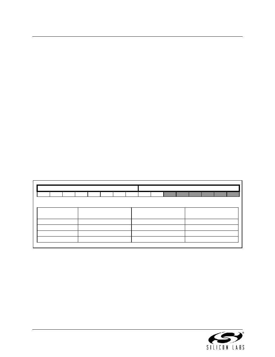
The IDAC data registers (IDA0H and IDA0L) are left-justified, meaning that the eight MSBs of the IDAC
output word are mapped to bits 7–0 of the IDA0H register, and the two LSBs of the IDAC output word are
mapped to bits 7 and 6 of the IDA0L register. The data word mapping for the IDAC is shown in Figure 6.2.
Figure 6.2. IDA0 Data Word Mapping
The full-scale output current of the IDAC is selected using the IDA0OMD bits (IDA0CN[1:0]). By default,
the IDAC is set to a full-scale output current of 2 mA. The IDA0OMD bits can also be configured to provide
full-scale output currents of 1 mA or 0.5 mA, as shown in SFR Definition 6.1.
IDA0H
IDA0L
D9
D8
D7
D6
D5
D4
D3
D2
D1
D0
Input Data Word
(D9–D0)
Output Current
IDA0OMD[1:0] = ‘1x’
Output Current
IDA0OMD[1:0] = ‘01’
Output Current
IDA0OMD[1:0] = ‘00’
0x000
0 mA
0x001
1/1024 x 2 mA
1/1024 x 1 mA
1/1024 x 0.5 mA
0x200
512/1024 x 2 mA
512/1024 x 1 mA
512/1024 x 0.5 mA
0x3FF
1023/1024 x 2 mA
1023/1024 x 1 mA
1023/1024 x 0.5 mA
相关PDF资料 |
PDF描述 |
|---|---|
| LGU2G101MELA | CAP ALUM 100UF 400V 20% SNAP |
| SDR-Q | SCOTCH CODE REFILL Q |
| 0210391036 | CABLE JUMPER 1MM .102M 33POS |
| RBM22DSXH | CONN EDGECARD 44POS DIP .156 SLD |
| C8051F310-TB | BOARD PROTOTYPING W/C8051F310 |
相关代理商/技术参数 |
参数描述 |
|---|---|
| C8051F330-TB-K | 功能描述:BOARD PROTOTYPING W/C8051F330 制造商:silicon labs 系列:- 零件状态:在售 板类型:评估平台 类型:MCU 8-位 核心处理器:8051 操作系统:- 平台:- 配套使用产品/相关产品:C8051F33x 安装类型:固定 内容:板 标准包装:1 |
| C8051F331 | 功能描述:8位微控制器 -MCU 8KB RoHS:否 制造商:Silicon Labs 核心:8051 处理器系列:C8051F39x 数据总线宽度:8 bit 最大时钟频率:50 MHz 程序存储器大小:16 KB 数据 RAM 大小:1 KB 片上 ADC:Yes 工作电源电压:1.8 V to 3.6 V 工作温度范围:- 40 C to + 105 C 封装 / 箱体:QFN-20 安装风格:SMD/SMT |
| C8051F331-GM | 功能描述:8位微控制器 -MCU 8KB 20P MCU RoHS:否 制造商:Silicon Labs 核心:8051 处理器系列:C8051F39x 数据总线宽度:8 bit 最大时钟频率:50 MHz 程序存储器大小:16 KB 数据 RAM 大小:1 KB 片上 ADC:Yes 工作电源电压:1.8 V to 3.6 V 工作温度范围:- 40 C to + 105 C 封装 / 箱体:QFN-20 安装风格:SMD/SMT |
| C8051F331-GMR | 功能描述:8位微控制器 -MCU 8KB 20P MCU on Tape and Reel RoHS:否 制造商:Silicon Labs 核心:8051 处理器系列:C8051F39x 数据总线宽度:8 bit 最大时钟频率:50 MHz 程序存储器大小:16 KB 数据 RAM 大小:1 KB 片上 ADC:Yes 工作电源电压:1.8 V to 3.6 V 工作温度范围:- 40 C to + 105 C 封装 / 箱体:QFN-20 安装风格:SMD/SMT |
| C8051F331R | 功能描述:8位微控制器 -MCU 8KB 20P MCU on Tape and Reel RoHS:否 制造商:Silicon Labs 核心:8051 处理器系列:C8051F39x 数据总线宽度:8 bit 最大时钟频率:50 MHz 程序存储器大小:16 KB 数据 RAM 大小:1 KB 片上 ADC:Yes 工作电源电压:1.8 V to 3.6 V 工作温度范围:- 40 C to + 105 C 封装 / 箱体:QFN-20 安装风格:SMD/SMT |
发布紧急采购,3分钟左右您将得到回复。