- 您现在的位置:买卖IC网 > PDF目录17090 > C8051F350-TB (Silicon Laboratories Inc)PROTOTYPINGBOARDWITH C8051F350 PDF资料下载
参数资料
| 型号: | C8051F350-TB |
| 厂商: | Silicon Laboratories Inc |
| 文件页数: | 47/234页 |
| 文件大小: | 0K |
| 描述: | PROTOTYPINGBOARDWITH C8051F350 |
| 标准包装: | 1 |
| 类型: | MCU |
| 适用于相关产品: | C8051F350 |
| 所含物品: | 板 |
第1页第2页第3页第4页第5页第6页第7页第8页第9页第10页第11页第12页第13页第14页第15页第16页第17页第18页第19页第20页第21页第22页第23页第24页第25页第26页第27页第28页第29页第30页第31页第32页第33页第34页第35页第36页第37页第38页第39页第40页第41页第42页第43页第44页第45页第46页当前第47页第48页第49页第50页第51页第52页第53页第54页第55页第56页第57页第58页第59页第60页第61页第62页第63页第64页第65页第66页第67页第68页第69页第70页第71页第72页第73页第74页第75页第76页第77页第78页第79页第80页第81页第82页第83页第84页第85页第86页第87页第88页第89页第90页第91页第92页第93页第94页第95页第96页第97页第98页第99页第100页第101页第102页第103页第104页第105页第106页第107页第108页第109页第110页第111页第112页第113页第114页第115页第116页第117页第118页第119页第120页第121页第122页第123页第124页第125页第126页第127页第128页第129页第130页第131页第132页第133页第134页第135页第136页第137页第138页第139页第140页第141页第142页第143页第144页第145页第146页第147页第148页第149页第150页第151页第152页第153页第154页第155页第156页第157页第158页第159页第160页第161页第162页第163页第164页第165页第166页第167页第168页第169页第170页第171页第172页第173页第174页第175页第176页第177页第178页第179页第180页第181页第182页第183页第184页第185页第186页第187页第188页第189页第190页第191页第192页第193页第194页第195页第196页第197页第198页第199页第200页第201页第202页第203页第204页第205页第206页第207页第208页第209页第210页第211页第212页第213页第214页第215页第216页第217页第218页第219页第220页第221页第222页第223页第224页第225页第226页第227页第228页第229页第230页第231页第232页第233页第234页
C8051F350/1/2/3
140
Rev. 1.1
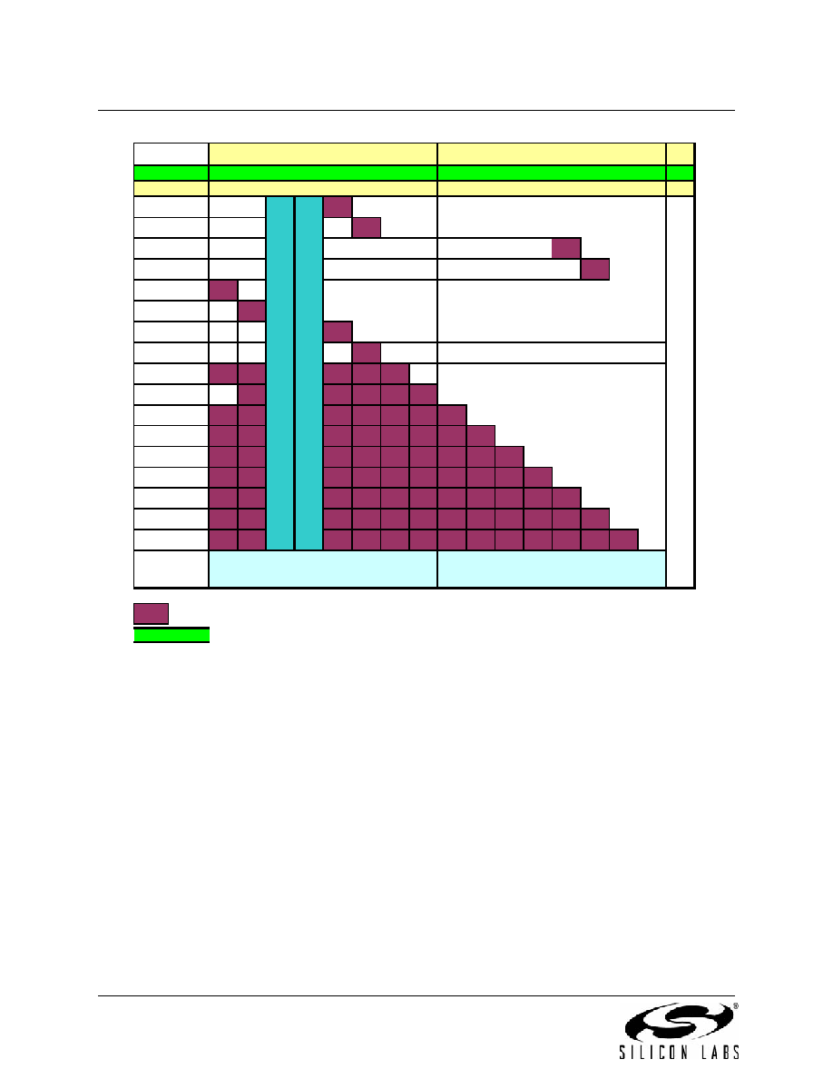
Figure 18.4. Crossbar Priority Decoder with Crystal Pins Skipped
Registers XBR0 and XBR1 are used to assign the digital I/O resources to the physical I/O Port pins. Note
that when the SMBus is selected, the Crossbar assigns both pins associated with the SMBus (SDA and
SCL); when the UART is selected, the Crossbar assigns both pins associated with the UART (TX and RX).
UART0 pin assignments are fixed for bootloading purposes: UART TX0 is always assigned to P0.4; UART
RX0 is always assigned to P0.5. Comparator outputs are also fixed: CP0A will appear only on P1.4, CP0
will appear only on P1.5. Standard Port I/Os appear contiguously after the prioritized functions have been
assigned.
Important Note: The SPI can be operated in either 3-wire or 4-wire modes, pending the state of the
NSSMD1–NSSMD0 bits in register SPI0CN. According to the SPI mode, the NSS signal may or may not
be routed to a Port pin.
P2
x1
x2
CNVSTR
IDA0 IDA1
01234567012345670
(*4-Wire SPI Only)
/SYSCLK
CEX0
CEX1
CEX2
ECI
0011000000000000
P0
P1
MISO
CP0A
CP0
SCK
RX0
SF Signals
PIN I/O
TX0
SDA
MOSI
NSS*
SCL
Special Function Signals are not assigned by the crossbar.
When these signals are enabled, the CrossBar must be
manually configured to skip their corresponding port pins.
Port pin potentially assignable to peripheral
SF Signals
T1
P0SKIP[0:7]
T0
P1SKIP[0:7]
相关PDF资料 |
PDF描述 |
|---|---|
| GEM25DTKT-S288 | CONN EDGECARD 50POS .156 EXTEND |
| RMC07DRXI | CONN EDGECARD 14POS DIP .100 SLD |
| VI-BT0-EY | CONVERTER MOD DC/DC 5V 50W |
| SDR-40-49 | SCOTCH CODE REFILL # 40-49 |
| EBC17DRAI | CONN EDGECARD 34POS R/A .100 SLD |
相关代理商/技术参数 |
参数描述 |
|---|---|
| C8051F350-TB-K | 功能描述:PROTOTYPINGBOARDWITH C8051F350 制造商:silicon labs 系列:- 零件状态:在售 板类型:评估平台 类型:MCU 8-位 核心处理器:8051 操作系统:- 平台:- 配套使用产品/相关产品:C8051F35x 安装类型:固定 内容:板 标准包装:1 |
| C8051F351 | 功能描述:8位微控制器 -MCU 24-bit ADC RoHS:否 制造商:Silicon Labs 核心:8051 处理器系列:C8051F39x 数据总线宽度:8 bit 最大时钟频率:50 MHz 程序存储器大小:16 KB 数据 RAM 大小:1 KB 片上 ADC:Yes 工作电源电压:1.8 V to 3.6 V 工作温度范围:- 40 C to + 105 C 封装 / 箱体:QFN-20 安装风格:SMD/SMT |
| C8051F351GM | 制造商:Silicon Laboratories Inc 功能描述: |
| C8051F351-GM | 功能描述:8位微控制器 -MCU 24-bit ADC RoHS:否 制造商:Silicon Labs 核心:8051 处理器系列:C8051F39x 数据总线宽度:8 bit 最大时钟频率:50 MHz 程序存储器大小:16 KB 数据 RAM 大小:1 KB 片上 ADC:Yes 工作电源电压:1.8 V to 3.6 V 工作温度范围:- 40 C to + 105 C 封装 / 箱体:QFN-20 安装风格:SMD/SMT |
| C8051F351-GMR | 功能描述:8位微控制器 -MCU 24-bit ADC RoHS:否 制造商:Silicon Labs 核心:8051 处理器系列:C8051F39x 数据总线宽度:8 bit 最大时钟频率:50 MHz 程序存储器大小:16 KB 数据 RAM 大小:1 KB 片上 ADC:Yes 工作电源电压:1.8 V to 3.6 V 工作温度范围:- 40 C to + 105 C 封装 / 箱体:QFN-20 安装风格:SMD/SMT |
发布紧急采购,3分钟左右您将得到回复。