- 您现在的位置:买卖IC网 > PDF目录3794 > C8051F362-GM (Silicon Laboratories Inc)IC 8051 MCU 32K FLASH 28QFN PDF资料下载
参数资料
| 型号: | C8051F362-GM |
| 厂商: | Silicon Laboratories Inc |
| 文件页数: | 88/288页 |
| 文件大小: | 0K |
| 描述: | IC 8051 MCU 32K FLASH 28QFN |
| 产品培训模块: | Serial Communication Overview |
| 标准包装: | 73 |
| 系列: | C8051F36x |
| 核心处理器: | 8051 |
| 芯体尺寸: | 8-位 |
| 速度: | 100MHz |
| 连通性: | SMBus(2 线/I²C),SPI,UART/USART |
| 外围设备: | POR,PWM,温度传感器,WDT |
| 输入/输出数: | 25 |
| 程序存储器容量: | 32KB(32K x 8) |
| 程序存储器类型: | 闪存 |
| RAM 容量: | 1K x 8 |
| 电压 - 电源 (Vcc/Vdd): | 3 V ~ 3.6 V |
| 数据转换器: | A/D 17x10b; D/A 1x10b |
| 振荡器型: | 内部 |
| 工作温度: | -40°C ~ 85°C |
| 封装/外壳: | 28-VFQFN 裸露焊盘 |
| 包装: | 管件 |
| 配用: | 336-1410-ND - KIT DEV FOR C8051F360 FAMILY |
| 其它名称: | 336-1409-5 |
第1页第2页第3页第4页第5页第6页第7页第8页第9页第10页第11页第12页第13页第14页第15页第16页第17页第18页第19页第20页第21页第22页第23页第24页第25页第26页第27页第28页第29页第30页第31页第32页第33页第34页第35页第36页第37页第38页第39页第40页第41页第42页第43页第44页第45页第46页第47页第48页第49页第50页第51页第52页第53页第54页第55页第56页第57页第58页第59页第60页第61页第62页第63页第64页第65页第66页第67页第68页第69页第70页第71页第72页第73页第74页第75页第76页第77页第78页第79页第80页第81页第82页第83页第84页第85页第86页第87页当前第88页第89页第90页第91页第92页第93页第94页第95页第96页第97页第98页第99页第100页第101页第102页第103页第104页第105页第106页第107页第108页第109页第110页第111页第112页第113页第114页第115页第116页第117页第118页第119页第120页第121页第122页第123页第124页第125页第126页第127页第128页第129页第130页第131页第132页第133页第134页第135页第136页第137页第138页第139页第140页第141页第142页第143页第144页第145页第146页第147页第148页第149页第150页第151页第152页第153页第154页第155页第156页第157页第158页第159页第160页第161页第162页第163页第164页第165页第166页第167页第168页第169页第170页第171页第172页第173页第174页第175页第176页第177页第178页第179页第180页第181页第182页第183页第184页第185页第186页第187页第188页第189页第190页第191页第192页第193页第194页第195页第196页第197页第198页第199页第200页第201页第202页第203页第204页第205页第206页第207页第208页第209页第210页第211页第212页第213页第214页第215页第216页第217页第218页第219页第220页第221页第222页第223页第224页第225页第226页第227页第228页第229页第230页第231页第232页第233页第234页第235页第236页第237页第238页第239页第240页第241页第242页第243页第244页第245页第246页第247页第248页第249页第250页第251页第252页第253页第254页第255页第256页第257页第258页第259页第260页第261页第262页第263页第264页第265页第266页第267页第268页第269页第270页第271页第272页第273页第274页第275页第276页第277页第278页第279页第280页第281页第282页第283页第284页第285页第286页第287页第288页
C8051F360/1/2/3/4/5/6/7/8/9
178
Rev. 1.0
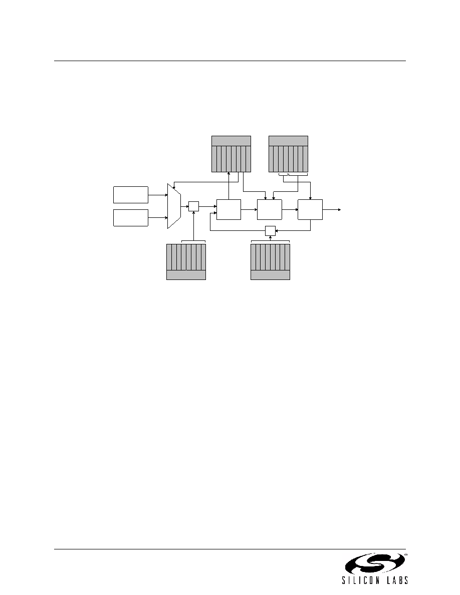
16.8. Phase-Locked Loop (PLL)
A Phase-Locked-Loop (PLL) is included, which is used to multiply the internal oscillator or an external
clock source to achieve higher CPU operating frequencies. The PLL circuitry is designed to produce an
output frequency between 25 MHz and 100 MHz, from a divided reference frequency between 5 MHz and
30 MHz. A block diagram of the PLL is shown in Figure 16.3.
PLL0DIV
PL
L
M
4
PL
L
M
3
PL
L
M
2
PL
L
M
1
PL
L
M
0
PLL0MUL
PLL
N
7
PLL
N
6
PLL
N
5
PLL
N
4
PLL
N
3
PLL
N
2
PLL
N
1
PLL
N
0
PLL0CN
PLLLCK
PLLSRC
PLLEN
PL
L
P
WR
PLL0FLT
PL
L
ICO
1
PL
L
ICO
0
P
L
LLP3
P
L
LLP2
P
L
LLP1
P
L
LLP0
0
1
Internal
Oscillator
External
Oscillator
÷
Phase /
Frequency
Detection
÷
Loop Filter
Current
Controlled
Oscillator
PLL Clock
Output
Divided
Reference
Clock
Figure 16.3. PLL Block Diagram
16.8.1. PLL Input Clock and Pre-divider
The PLL circuitry can derive its reference clock from either the internal oscillator or an external clock
source. The PLLSRC bit (PLL0CN.2) controls which clock source is used for the reference clock (see SFR
Definition 16.6). If PLLSRC is set to ‘0’, the internal oscillator source is used. Note that the internal oscilla-
tor divide factor (as specified by bits IFCN1-0 in register OSCICN) will also apply to this clock. When
PLLSRC is set to ‘1’, an external oscillator source will be used. The external oscillator should be active and
settled before it is selected as a reference clock for the PLL circuit. The reference clock is divided down
prior to the PLL circuit, according to the contents of the PLLM4-0 bits in the PLL Pre-divider Register
(PLL0DIV), shown in SFR Definition 16.7.
16.8.2. PLL Multiplication and Output Clock
The PLL circuitry will multiply the divided reference clock by the multiplication factor stored in the
PLL0MUL register shown in SFR Definition 16.8. To accomplish this, it uses a feedback loop consisting of
a phase/frequency detector, a loop filter, and a current-controlled oscillator (ICO). It is important to config-
ure the loop filter and the ICO for the correct frequency ranges. The PLLLP3–0 bits (PLL0FLT.3–0) should
be set according to the divided reference clock frequency. Likewise, the PLLICO1–0 bits (PLL0FLT.5–4)
should be set according to the desired output frequency range. SFR Definition 16.9 describes the proper
settings to use for the PLLLP3–0 and PLLICO1–0 bits. When the PLL is locked and stable at the desired
frequency, the PLLLCK bit (PLL0CN.5) will be set to a ‘1’. The resulting PLL frequency will be set accord-
ing to the equation:
PLL Frequency
Reference Frequency
PLLN
PLLM
---------------
×
=
Where “Reference Frequency” is the selected source clock frequency, PLLN is the PLL Multiplier, and
PLLM is the PLL Pre-divider.
相关PDF资料 |
PDF描述 |
|---|---|
| MC68332ACPV16 | IC MCU 32BIT 16MHZ AMASK 144LQFP |
| MC68HC908QY4CDT | IC MCU 4K FLASH W/ADC 16-TSSOP |
| C8051F366-GQ | IC 8051 MCU 32K FLASH 32-LQFP |
| MC68HC908QY4CDW | IC MCU 4K FLASH W/ADC 16-SOIC |
| MC68HC908QY4CP | IC MCU 4K FLASH W/ADC 16-DIP |
相关代理商/技术参数 |
参数描述 |
|---|---|
| C8051F362-GM2 | 制造商:SILABS 制造商全称:SILABS 功能描述:Mixed Signal ISP Flash MCU Family |
| C8051F362-GMR | 功能描述:8位微控制器 -MCU 32KB 100MIPS 10ADC 10DAC 28Pin MCU RoHS:否 制造商:Silicon Labs 核心:8051 处理器系列:C8051F39x 数据总线宽度:8 bit 最大时钟频率:50 MHz 程序存储器大小:16 KB 数据 RAM 大小:1 KB 片上 ADC:Yes 工作电源电压:1.8 V to 3.6 V 工作温度范围:- 40 C to + 105 C 封装 / 箱体:QFN-20 安装风格:SMD/SMT |
| C8051F363 | 制造商:SILABS 制造商全称:SILABS 功能描述:Mixed Signal ISP Flash MCU Family |
| C8051F363-C-GQ | 功能描述:8051 C8051F36x Microcontroller IC 8-Bit 100MHz 32KB (32K x 8) FLASH 48-TQFP (7x7) 制造商:silicon labs 系列:C8051F36x 包装:托盘 零件状态:Not For New Designs 核心处理器:8051 核心尺寸:8-位 速度:100MHz 连接性:EBI/EMI,SMBus(2 线/I2C),SPI,UART/USART 外设:POR,PWM,WDT I/O 数:39 程序存储容量:32KB(32K x 8) 程序存储器类型:闪存 EEPROM 容量:- RAM 容量:1K x 8 电压 - 电源(Vcc/Vdd):3 V ~ 3.6 V 数据转换器:- 振荡器类型:内部 工作温度:-40°C ~ 85°C(TA) 封装/外壳:48-TQFP 供应商器件封装:48-TQFP(7x7) 标准包装:250 |
| C8051F363-C-GQR | 功能描述:8051 C8051F36x Microcontroller IC 8-Bit 100MHz 32KB (32K x 8) FLASH 48-TQFP (7x7) 制造商:silicon labs 系列:C8051F36x 包装:带卷(TR) 零件状态:Not For New Designs 核心处理器:8051 核心尺寸:8-位 速度:100MHz 连接性:EBI/EMI,SMBus(2 线/I2C),SPI,UART/USART 外设:POR,PWM,WDT I/O 数:39 程序存储容量:32KB(32K x 8) 程序存储器类型:闪存 EEPROM 容量:- RAM 容量:1K x 8 电压 - 电源(Vcc/Vdd):3 V ~ 3.6 V 数据转换器:- 振荡器类型:内部 工作温度:-40°C ~ 85°C(TA) 封装/外壳:48-TQFP 供应商器件封装:48-TQFP(7x7) 标准包装:500 |
发布紧急采购,3分钟左右您将得到回复。