参数资料
| 型号: | C8051T631-GM |
| 厂商: | Silicon Laboratories Inc |
| 文件页数: | 26/220页 |
| 文件大小: | 0K |
| 描述: | IC MCU 8KB 20PIN QFN |
| 产品培训模块: | Serial Communication Overview |
| 标准包装: | 91 |
| 系列: | C8051T63x |
| 核心处理器: | 8051 |
| 芯体尺寸: | 8-位 |
| 速度: | 25MHz |
| 连通性: | SMBus(2 线/I²C),SPI,UART/USART |
| 外围设备: | POR,PWM,WDT |
| 输入/输出数: | 17 |
| 程序存储器容量: | 8KB(8K x 8) |
| 程序存储器类型: | OTP |
| RAM 容量: | 768 x 8 |
| 电压 - 电源 (Vcc/Vdd): | 1.8 V ~ 3.6 V |
| 振荡器型: | 内部 |
| 工作温度: | -40°C ~ 85°C |
| 封装/外壳: | 20-VFQFN 裸露焊盘 |
| 包装: | 管件 |
| 配用: | 336-1464-ND - KIT DEV FOR C8051T630 FAMILY |
| 其它名称: | 336-1459-5 |
第1页第2页第3页第4页第5页第6页第7页第8页第9页第10页第11页第12页第13页第14页第15页第16页第17页第18页第19页第20页第21页第22页第23页第24页第25页当前第26页第27页第28页第29页第30页第31页第32页第33页第34页第35页第36页第37页第38页第39页第40页第41页第42页第43页第44页第45页第46页第47页第48页第49页第50页第51页第52页第53页第54页第55页第56页第57页第58页第59页第60页第61页第62页第63页第64页第65页第66页第67页第68页第69页第70页第71页第72页第73页第74页第75页第76页第77页第78页第79页第80页第81页第82页第83页第84页第85页第86页第87页第88页第89页第90页第91页第92页第93页第94页第95页第96页第97页第98页第99页第100页第101页第102页第103页第104页第105页第106页第107页第108页第109页第110页第111页第112页第113页第114页第115页第116页第117页第118页第119页第120页第121页第122页第123页第124页第125页第126页第127页第128页第129页第130页第131页第132页第133页第134页第135页第136页第137页第138页第139页第140页第141页第142页第143页第144页第145页第146页第147页第148页第149页第150页第151页第152页第153页第154页第155页第156页第157页第158页第159页第160页第161页第162页第163页第164页第165页第166页第167页第168页第169页第170页第171页第172页第173页第174页第175页第176页第177页第178页第179页第180页第181页第182页第183页第184页第185页第186页第187页第188页第189页第190页第191页第192页第193页第194页第195页第196页第197页第198页第199页第200页第201页第202页第203页第204页第205页第206页第207页第208页第209页第210页第211页第212页第213页第214页第215页第216页第217页第218页第219页第220页
Rev. 1.0
121
C8051T630/1/2/3/4/5
20.6. Special Function Registers for Accessing and Configuring Port I/O
All Port I/O are accessed through corresponding special function registers (SFRs) that are both byte
addressable and bit addressable. When writing to a Port, the value written to the SFR is latched to main-
tain the output data value at each pin. When reading, the logic levels of the Port's input pins are returned
regardless of the XBRn settings (i.e., even when the pin is assigned to another signal by the Crossbar, the
Port register can always read its corresponding Port I/O pin). The exception to this is the execution of the
read-modify-write instructions that target a Port Latch register as the destination. The read-modify-write
instructions when operating on a Port SFR are the following: ANL, ORL, XRL, JBC, CPL, INC, DEC, DJNZ
and MOV, CLR or SETB, when the destination is an individual bit in a Port SFR. For these instructions, the
value of the latch register (not the pin) is read, modified, and written back to the SFR.
Each Port has a corresponding PnSKIP register which allows its individual Port pins to be assigned to dig-
ital functions or skipped by the Crossbar. All Port pins used for analog functions, GPIO, or dedicated digital
functions such as the EMIF should have their PnSKIP bit set to 1.
The Port input mode of the I/O pins is defined using the Port Input Mode registers (PnMDIN). Each Port
cell can be configured for analog or digital I/O. This selection is required even for the digital resources
selected in the XBRn registers, and is not automatic. The only exception to this is P2.4, which can only be
used for digital I/O.
The output driver characteristics of the I/O pins are defined using the Port Output Mode registers (PnMD-
OUT). Each Port Output driver can be configured as either open drain or push-pull. This selection is
required even for the digital resources selected in the XBRn registers, and is not automatic. The only
exception to this is the SMBus (SDA, SCL) pins, which are configured as open-drain regardless of the
PnMDOUT settings.
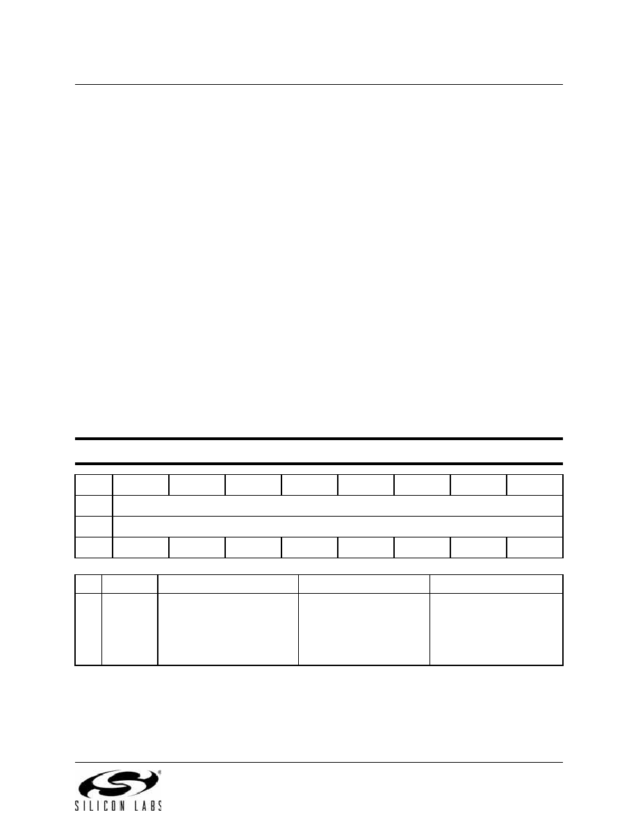
SFR Address = 0x80; Bit-Addressable
SFR Definition 20.7. P0: Port 0
Bit
76543210
Name
P0[7:0]
Type
R/W
Reset
11111111
Bit
Name
Description
Write
Read
7:0
P0[7:0]
Port 0 Data.
Sets the Port latch logic
value or reads the Port pin
logic state in Port cells con-
figured for digital I/O.
0: Set output latch to logic
LOW.
1: Set output latch to logic
HIGH.
0: P0.n Port pin is logic
LOW.
1: P0.n Port pin is logic
HIGH.
相关PDF资料 |
PDF描述 |
|---|---|
| C88F83B0AU-TC-H | MCU 16BIT 256K LCD 120-TQFP |
| CAT5112VI-10-T3 | IC POT DIGITL 10K 32TAP 8SOIC |
| CAT5113ZI01 | IC POT DPP NV 100TAP U/D 8MSOP |
| CAT5115ZI-50-G | IC POT DIG 50K 32TAP 8MSOP |
| CAT5116LI-G | IC POT DIG LOG 32K 100TAP 8DIP |
相关代理商/技术参数 |
参数描述 |
|---|---|
| C8051T631-GMR | 功能描述:8位微控制器 -MCU 8KB 20Pin MCU RoHS:否 制造商:Silicon Labs 核心:8051 处理器系列:C8051F39x 数据总线宽度:8 bit 最大时钟频率:50 MHz 程序存储器大小:16 KB 数据 RAM 大小:1 KB 片上 ADC:Yes 工作电源电压:1.8 V to 3.6 V 工作温度范围:- 40 C to + 105 C 封装 / 箱体:QFN-20 安装风格:SMD/SMT |
| C8051T632-GM | 功能描述:8位微控制器 -MCU 4KB 10ADC DAC10 20 Pin MCU RoHS:否 制造商:Silicon Labs 核心:8051 处理器系列:C8051F39x 数据总线宽度:8 bit 最大时钟频率:50 MHz 程序存储器大小:16 KB 数据 RAM 大小:1 KB 片上 ADC:Yes 工作电源电压:1.8 V to 3.6 V 工作温度范围:- 40 C to + 105 C 封装 / 箱体:QFN-20 安装风格:SMD/SMT |
| C8051T632-GMR | 功能描述:8位微控制器 -MCU 4KB 10ADC DAC10 20 Pin MCU RoHS:否 制造商:Silicon Labs 核心:8051 处理器系列:C8051F39x 数据总线宽度:8 bit 最大时钟频率:50 MHz 程序存储器大小:16 KB 数据 RAM 大小:1 KB 片上 ADC:Yes 工作电源电压:1.8 V to 3.6 V 工作温度范围:- 40 C to + 105 C 封装 / 箱体:QFN-20 安装风格:SMD/SMT |
| C8051T633-GM | 功能描述:8位微控制器 -MCU 4KB 20Pin MCU RoHS:否 制造商:Silicon Labs 核心:8051 处理器系列:C8051F39x 数据总线宽度:8 bit 最大时钟频率:50 MHz 程序存储器大小:16 KB 数据 RAM 大小:1 KB 片上 ADC:Yes 工作电源电压:1.8 V to 3.6 V 工作温度范围:- 40 C to + 105 C 封装 / 箱体:QFN-20 安装风格:SMD/SMT |
| C8051T633-GMR | 功能描述:8位微控制器 -MCU 4KB 20Pin MCU RoHS:否 制造商:Silicon Labs 核心:8051 处理器系列:C8051F39x 数据总线宽度:8 bit 最大时钟频率:50 MHz 程序存储器大小:16 KB 数据 RAM 大小:1 KB 片上 ADC:Yes 工作电源电压:1.8 V to 3.6 V 工作温度范围:- 40 C to + 105 C 封装 / 箱体:QFN-20 安装风格:SMD/SMT |
发布紧急采购,3分钟左右您将得到回复。