- 您现在的位置:买卖IC网 > PDF目录10779 > CA3338AE (Intersil)IC CONV D/A R2R CMOS 8-BIT 16DIP PDF资料下载
参数资料
| 型号: | CA3338AE |
| 厂商: | Intersil |
| 文件页数: | 6/10页 |
| 文件大小: | 0K |
| 描述: | IC CONV D/A R2R CMOS 8-BIT 16DIP |
| 标准包装: | 25 |
| 设置时间: | 20ns |
| 位数: | 8 |
| 数据接口: | 并联 |
| 转换器数目: | 1 |
| 电压电源: | 单电源 |
| 工作温度: | -40°C ~ 85°C |
| 安装类型: | 通孔 |
| 封装/外壳: | 16-DIP(0.300",7.62mm) |
| 供应商设备封装: | 16-PDIP |
| 包装: | 管件 |
| 输出数目和类型: | 1 电压,单极;1 电压,双极 |
| 采样率(每秒): | 50M |
| 其它名称: | CA3338 CA338 |
5
CA3338, CA3338A
Digital Signal Path
The digital inputs (LE, COMP, and D0 - D7) are of TTL
compatible HCT High Speed CMOS design: the loading is
essentially capacitive and the logic threshold is typically
1.5V.
The 8 data bits, D0 (weighted 20) through D7 (weighted 27),
are applied to Exclusive OR gates (see Functional Diagram).
The COMP (data complement) control provides the second
input to the gates: if COMP is high, the data bits will be
inverted as they pass through.
The input data and the LE (latch enable) signals are next
applied to a level shifter. The inputs, operating between the
levels of VDD and VSS, are shifted to operate between VDD
and VEE. VEE optionally at ground or at a negative voltage,
will be discussed under bipolar operation. All further logic
elements except the output drivers operate from the VDD
and VEE supplies.
The upper 3 bits of data, D5 through D7, are input to a 3-to-7
line bar graph encoder. The encoder outputs and D0 through
D4 are applied to a feedthrough latch, which is controlled by
LE (latch enable).
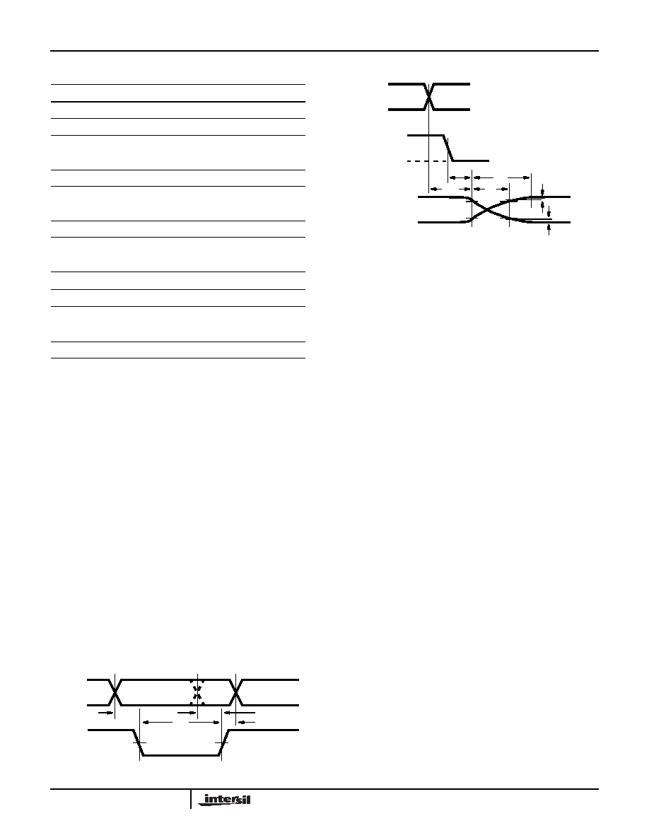
Latch Operation
Data is fed from input to output while LE is low: LE should be
tied low for non-clocked operation.
Non-clocked operation or changing data while LE is low is
not recommended for applications requiring low output
“glitch” energy: there is no guarantee of the simultaneous
changing of input data or the equal propagation delay of all
bits through the converter. Several parameters are given if
the converter is to be used in either of these modes: tD2
gives the delay from the input changing to the output
changing (10%), while tSU2 and tH give the set up and hold
times (referred to LE rising edge) needed to latch data. See
Figures 1 and 2.
Clocked operation is needed for low “glitch” energy use. Data
must meet the given tSU1 set up time to the LE falling edge,
and the tH hold time from the LE rising edge. The delay to
the output changing, tD1, is now referred to the LE falling
edge.
There is no need for a square wave LE clock; LE must only
meet the minimum tW pulse width for successful latch
operation. Generally, output timing (desired accuracy of
settling) sets the upper limit of usable clock frequency.
Output Structure
The latches feed data to a row of high current CMOS drivers,
which in turn feed a modified R2R ladder network.
The “N” channel (pull down) transistor of each driver plus the
bottom “2R” resistor are returned to VREF- this is the (-) full-
scale reference. The “P” channel (pull up) transistor of each
driver is returned to VREF+, the (+) full-scale reference.
In unipolar operation, VREF- would typically be returned to
analog ground, but may be raised above ground (see
specifications). There is substantial code dependent current
that flows from VREF+ to VREF- (see VREF+ input current in
specifications), so VREF- should have a low impedance path
to ground.
Pin Descriptions
PIN
NAME
DESCRIPTION
1
D7
Most Significant Bit
2
D6
Input
3D5
Data
4D4
Bits
5
D3
(High = True)
6D2
7D1
8VSS
Digital Ground
9D
0
Least Significant Bit. Input Data Bit
10
VEE
Analog Ground
11
VREF- Reference Voltage Negative Input
12
VOUT
Analog Output
13
VREF+ Reference Voltage Positive Input
14
COMP
Data Complement Control input. Active High
15
LE
Latch Enable Input. Active Low
16
V
DD
Digital Power Supply, +5V
INPUT DATA
LATCH
tSU1
tSU2
tW
tH
ENABLE
LATCHED
DATA
FEEDTHROUGH
FIGURE 1. DATA TO LATCH ENABLE TIMING
tD1
tD2
tr
tS
1/
2 LSB
1/
2 LSB
90%
10%
INPUT
LATCH
ENABLE
OUTPUT
VOLTAGE
DATA
FIGURE 2. DATA AND LATCH ENABLE TO OUTPUT TIMING
相关PDF资料 |
PDF描述 |
|---|---|
| VE-BWK-IV-S | CONVERTER MOD DC/DC 40V 150W |
| B37931K5152K060 | CAP CER 1500PF 50V 10% X7R 0603 |
| VE-B1W-IV-S | CONVERTER MOD DC/DC 5.5V 150W |
| JBXFE2G05MSSDSR | CONN PLUG 5POS SEAL IP67 SOLDER |
| B37931K5221K060 | CAP CER 220PF 50V 10% X7R 0603 |
相关代理商/技术参数 |
参数描述 |
|---|---|
| CA3338AEZ | 功能描述:数模转换器- DAC 16 INDTEMP VID D/A 8BIT 50MHZ 0 75 LSB RoHS:否 制造商:Texas Instruments 转换器数量:1 DAC 输出端数量:1 转换速率:2 MSPs 分辨率:16 bit 接口类型:QSPI, SPI, Serial (3-Wire, Microwire) 稳定时间:1 us 最大工作温度:+ 85 C 安装风格:SMD/SMT 封装 / 箱体:SOIC-14 封装:Tube |
| CA3338AM | 制造商:Rochester Electronics LLC 功能描述:16 SOIC(W) INDTEMP VIDEO D/A 8BIT 50MHZ 0.75 LSB - Bulk |
| CA3338AM96 | 制造商:Rochester Electronics LLC 功能描述:- Bulk |
| CA3338AMZ | 功能描述:数模转换器- DAC 16(W INDTEMP VID D/A 8BIT 50MHZ 0 75 LSB RoHS:否 制造商:Texas Instruments 转换器数量:1 DAC 输出端数量:1 转换速率:2 MSPs 分辨率:16 bit 接口类型:QSPI, SPI, Serial (3-Wire, Microwire) 稳定时间:1 us 最大工作温度:+ 85 C 安装风格:SMD/SMT 封装 / 箱体:SOIC-14 封装:Tube |
| CA3338AMZ96 | 功能描述:数模转换器- DAC 16(W INDTEMP VID D/A 8BIT 50MHZ 0 75 LSB RoHS:否 制造商:Texas Instruments 转换器数量:1 DAC 输出端数量:1 转换速率:2 MSPs 分辨率:16 bit 接口类型:QSPI, SPI, Serial (3-Wire, Microwire) 稳定时间:1 us 最大工作温度:+ 85 C 安装风格:SMD/SMT 封装 / 箱体:SOIC-14 封装:Tube |
发布紧急采购,3分钟左右您将得到回复。