- 您现在的位置:买卖IC网 > PDF目录10779 > CA3338AE (Intersil)IC CONV D/A R2R CMOS 8-BIT 16DIP PDF资料下载
参数资料
| 型号: | CA3338AE |
| 厂商: | Intersil |
| 文件页数: | 7/10页 |
| 文件大小: | 0K |
| 描述: | IC CONV D/A R2R CMOS 8-BIT 16DIP |
| 标准包装: | 25 |
| 设置时间: | 20ns |
| 位数: | 8 |
| 数据接口: | 并联 |
| 转换器数目: | 1 |
| 电压电源: | 单电源 |
| 工作温度: | -40°C ~ 85°C |
| 安装类型: | 通孔 |
| 封装/外壳: | 16-DIP(0.300",7.62mm) |
| 供应商设备封装: | 16-PDIP |
| 包装: | 管件 |
| 输出数目和类型: | 1 电压,单极;1 电压,双极 |
| 采样率(每秒): | 50M |
| 其它名称: | CA3338 CA338 |
6
CA3338, CA3338A
In bipolar operation, VREF- would be returned to a negative
voltage (the maximum voltage rating to VDD must be
observed). VEE, which supplies the gate potential for the
output drivers, must be returned to a point at least as
negative as VREF-. Note that the maximum clocking speed
decreases when the bipolar mode is used.
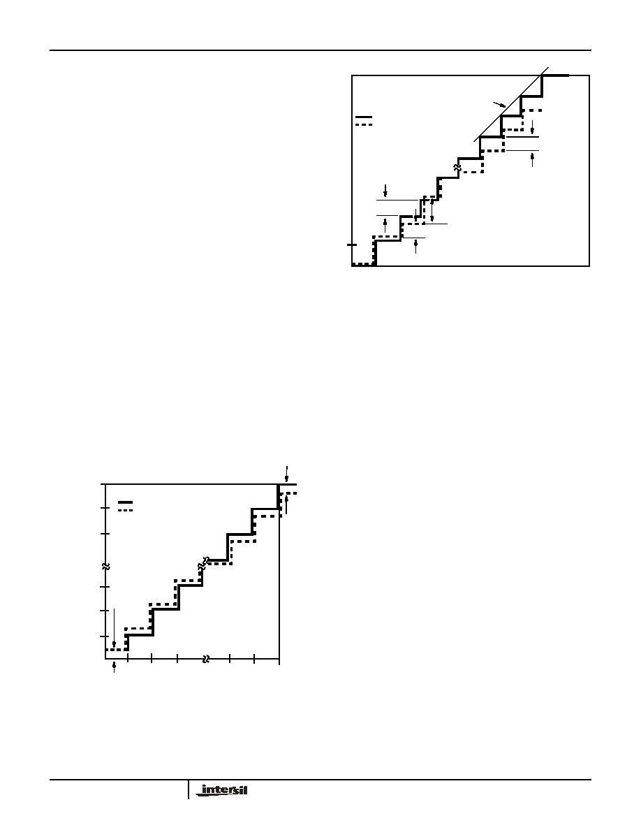
Static Characteristics
The ideal 8-bit D/A would have an output equal to VREF- with
an input code of 00HEX (zero scale output), and an output
equal to 255/256 of VREF+ (referred to VREF-) with an input
code of FFHEX (full scale output). The difference between the
ideal and actual values of these two parameters are the
OFFSET and GAIN errors, respectively; see Figure 3.
If the code into an 8-bit D/A is changed by 1 count, the output
should change by 1/255 (full scale output - zero scale output). A
deviation from this step size is a differential linearity error, see
Figure 4. Note that the error is expressed in fractions of the
ideal step size (usually called an LSB). Also note that if the (-)
differential linearity error is less (in absolute numbers) than 1
LSB, the device is monotonic. (The output will always increase
for increasing code or decrease for decreasing code).
If the code into an 8-bit D/A is at any value, say “N”, the output
voltage should be N/255 of the full scale output (referred to the
zero scale output). Any deviation from that output is an integral
linearity error, usually expressed in LSBs. See Figure 4.
Note that OFFSET and GAIN errors do not affect integral
linearity, as the linearity is referenced to actual zero and full
scale outputs, not ideal. Absolute accuracy would have to
also take these errors into account.
Dynamic Characteristics
Keeping the full-scale range (VREF+ - VREF-) as high as
possible gives the best linearity and lowest “glitch” energy
(referred to 1V). This provides the best “P” and “N” channel
gate drives (hence saturation resistance) and propagation
delays. The VREF+ (and VREF- if bipolar) terminal should be
well bypassed as near the chip as possible.
“Glitch” energy is defined as a spurious voltage that occurs as
the output is changed from one voltage to another. In a binary
input converter, it is usually highest at the most significant bit
transition (7FHEX to 80HEX for an 8 bit device), and can be
measured by displaying the output as the input code
alternates around that point. The “glitch” energy is the area
between the actual output display and an ideal one LSB step
voltage (subtracting negative area from positive), at either the
positive or negative-going step. It is usually expressed in pV/s.
The CA3338 uses a modified R2R ladder, where the 3 most
significant bits drive a bar graph decoder and 7 equally
weighted resistors. This makes the “glitch” energy at each 1/8
scale transition (1FHEX to 20HEX, 3FHEX to 40HEX, etc.)
essentially equal, and far less than the MSB transition would
otherwise display.
For the purpose of comparison to other converters, the output
should be resistively divided to 1V full scale. Figure 5 shows a
typical hook-up for checking “glitch” energy or settling time.
The settling time of the A/D is mainly a function of the output
resistance (approximately 160
in parallel with the load
resistance) and the load plus internal chip capacitance. Both
“glitch” energy and settling time measurements require very
good circuit and probe grounding: a probe tip connector such
as Tektronix part number 131-0258-00 is recommended.
255/256
254/256
253/256
3/256
2/256
1/256
0
00
01
02
03
FD
FE
FF
= IDEAL TRANSFER CURVE
= ACTUAL TRANSFER CURVE
OFFSET
ERROR
(SHOWN +)
OUTPUT
V
O
L
T
A
G
E
AS
A
FRA
C
TION
OF
V
REF
+
-
V
RE
F
-
GAIN ERROR
(SHOWN -)
INPUT CODE IN HEXADECIMAL (COMP = LOW)
FIGURE 3. D/A OFFSET AND GAIN ERROR
0
00
OUT
P
UT
V
O
L
T
A
G
E
C
B
FROM “0” SCALE
INTEGRAL LINEARITY
ERROR (SHOWN -)
STRAIGHT LINE
TO FULL SCALE
VOLTAGE
INPUT CODE
= IDEAL TRANSFER CURVE
= ACTUAL TRANSFER CURVE
A = IDEAL STEP SIZE (1/255 OF FULL
B - A = +DIFFERENTIAL LINEARITY ERROR
C - A = -DIFFERENTIAL LINEARITY ERROR
A
SCALE -“0” SCALE VOLTAGE)
FIGURE 4. D/A INTEGRAL AND DIFFERENTIAL LINEARITY
ERROR
相关PDF资料 |
PDF描述 |
|---|---|
| VE-BWK-IV-S | CONVERTER MOD DC/DC 40V 150W |
| B37931K5152K060 | CAP CER 1500PF 50V 10% X7R 0603 |
| VE-B1W-IV-S | CONVERTER MOD DC/DC 5.5V 150W |
| JBXFE2G05MSSDSR | CONN PLUG 5POS SEAL IP67 SOLDER |
| B37931K5221K060 | CAP CER 220PF 50V 10% X7R 0603 |
相关代理商/技术参数 |
参数描述 |
|---|---|
| CA3338AEZ | 功能描述:数模转换器- DAC 16 INDTEMP VID D/A 8BIT 50MHZ 0 75 LSB RoHS:否 制造商:Texas Instruments 转换器数量:1 DAC 输出端数量:1 转换速率:2 MSPs 分辨率:16 bit 接口类型:QSPI, SPI, Serial (3-Wire, Microwire) 稳定时间:1 us 最大工作温度:+ 85 C 安装风格:SMD/SMT 封装 / 箱体:SOIC-14 封装:Tube |
| CA3338AM | 制造商:Rochester Electronics LLC 功能描述:16 SOIC(W) INDTEMP VIDEO D/A 8BIT 50MHZ 0.75 LSB - Bulk |
| CA3338AM96 | 制造商:Rochester Electronics LLC 功能描述:- Bulk |
| CA3338AMZ | 功能描述:数模转换器- DAC 16(W INDTEMP VID D/A 8BIT 50MHZ 0 75 LSB RoHS:否 制造商:Texas Instruments 转换器数量:1 DAC 输出端数量:1 转换速率:2 MSPs 分辨率:16 bit 接口类型:QSPI, SPI, Serial (3-Wire, Microwire) 稳定时间:1 us 最大工作温度:+ 85 C 安装风格:SMD/SMT 封装 / 箱体:SOIC-14 封装:Tube |
| CA3338AMZ96 | 功能描述:数模转换器- DAC 16(W INDTEMP VID D/A 8BIT 50MHZ 0 75 LSB RoHS:否 制造商:Texas Instruments 转换器数量:1 DAC 输出端数量:1 转换速率:2 MSPs 分辨率:16 bit 接口类型:QSPI, SPI, Serial (3-Wire, Microwire) 稳定时间:1 us 最大工作温度:+ 85 C 安装风格:SMD/SMT 封装 / 箱体:SOIC-14 封装:Tube |
发布紧急采购,3分钟左右您将得到回复。