- 您现在的位置:买卖IC网 > PDF目录169496 > CAT28F001NI-12T 128K X 8 FLASH 12V PROM, 120 ns, PQCC32 PDF资料下载
参数资料
| 型号: | CAT28F001NI-12T |
| 元件分类: | PROM |
| 英文描述: | 128K X 8 FLASH 12V PROM, 120 ns, PQCC32 |
| 封装: | PLASTIC, LCC-32 |
| 文件页数: | 12/18页 |
| 文件大小: | 455K |
| 代理商: | CAT28F001NI-12T |
CAT28F001
3
Doc. No. 1078, Rev. I
ABSOLUTE MAXIMUM RATINGS*
Temperature Under Bias ................... –55
°C to +95°C
Storage Temperature ....................... –65
°C to +150°C
Voltage on Any Pin with
Respect to Ground(1) ........... –2.0V to +VCC + 2.0V
(Except A9, RP, OE, VCC and VPP)
Voltage on Pin A9, RP AND OE with
Respect to Ground(1) ................... –2.0V to +13.5V
VPP with Respect to Ground
during Program/Erase(1) .............. –2.0V to +14.0V
VCC with Respect to Ground(1) ............ –2.0V to +7.0V
Package Power Dissipation
Capability (TA = 25
°C) .................................. 1.0 W
Lead Soldering Temperature (10 secs) ............ 300
°C
Output Short Circuit Current(2) ........................ 100 mA
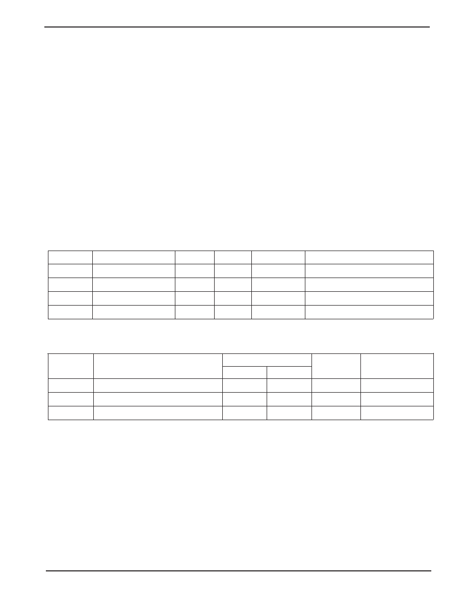
RELIABILITY CHARACTERISTICS
Symbol
Parameter
Min.
Max.
Units
Test Method
NEND(3)
Endurance
100K
Cycles/Byte
MIL-STD-883, Test Method 1033
TDR(3)
Data Retention
10
Years
MIL-STD-883, Test Method 1008
VZAP(3)
ESD Susceptibility
2000
Volts
MIL-STD-883, Test Method 3015
ILTH(3)(4)
Latch-Up
100
mA
JEDEC Standard 17
CAPACITANCE TA = 25°C, f = 1.0 MHz
Limits
Symbol
Test
Min
Max.
Units
Conditions
CIN(3)
Input Pin Capacitance
8
pF
VIN = 0V
COUT(3)
Output Pin Capacitance
12
pF
VOUT = 0V
CVPP(3)
VPP Supply Capacitance
25
pF
VPP = 0V
Note:
(1) The minimum DC input voltage is –0.5V. During transitions, inputs may undershoot to –2.0V for periods of less than 20 ns. Maximum DC
voltage on output pins is VCC +0.5V, which may overshoot to VCC + 2.0V for periods of less than 20ns.
(2) Output shorted for no more than one second. No more than one output shorted at a time.
(3) This parameter is tested initially and after a design or process change that affects the parameter.
(4) Latch-up protection is provided for stresses up to 100 mA on address and data pins from –1V to VCC +1V.
*COMMENT
Stresses above those listed under “Absolute Maximum
Ratings” may cause permanent damage to the device.
These are stress ratings only, and functional operation of
the device at these or any other conditions outside of those
listed in the operational sections of this specification is not
implied. Exposure to any absolute maximum rating for
extended periods may affect device performance and
reliability.
相关PDF资料 |
PDF描述 |
|---|---|
| CAT28F010GA-12 | 128K X 8 FLASH 12V PROM, 120 ns, PQCC32 |
| CAT28F010HRI-90 | 128K X 8 FLASH 12V PROM, 90 ns, PDSO32 |
| CAT28F010H14I-90TE13 | 128K X 8 FLASH 12V PROM, 90 ns, PDSO32 |
| CAT28F010TI-12TE13 | 128K X 8 FLASH 12V PROM, 120 ns, PDSO32 |
| CAT28F010TR-12TE7 | 128K X 8 FLASH 12V PROM, 120 ns, PDSO32 |
相关代理商/技术参数 |
参数描述 |
|---|---|
| CAT28F001NI-90B | 功能描述:闪存 (128x8) 1M RoHS:否 制造商:ON Semiconductor 数据总线宽度:1 bit 存储类型:Flash 存储容量:2 MB 结构:256 K x 8 定时类型: 接口类型:SPI 访问时间: 电源电压-最大:3.6 V 电源电压-最小:2.3 V 最大工作电流:15 mA 工作温度:- 40 C to + 85 C 安装风格:SMD/SMT 封装 / 箱体: 封装:Reel |
| CAT28F001NI-90T | 功能描述:闪存 (128x8) 1M RoHS:否 制造商:ON Semiconductor 数据总线宽度:1 bit 存储类型:Flash 存储容量:2 MB 结构:256 K x 8 定时类型: 接口类型:SPI 访问时间: 电源电压-最大:3.6 V 电源电压-最小:2.3 V 最大工作电流:15 mA 工作温度:- 40 C to + 85 C 安装风格:SMD/SMT 封装 / 箱体: 封装:Reel |
| CAT28F001P-12B | 功能描述:闪存 (128x8) 1M RoHS:否 制造商:ON Semiconductor 数据总线宽度:1 bit 存储类型:Flash 存储容量:2 MB 结构:256 K x 8 定时类型: 接口类型:SPI 访问时间: 电源电压-最大:3.6 V 电源电压-最小:2.3 V 最大工作电流:15 mA 工作温度:- 40 C to + 85 C 安装风格:SMD/SMT 封装 / 箱体: 封装:Reel |
| CAT28F001P-12T | 功能描述:闪存 (128x8) 1M RoHS:否 制造商:ON Semiconductor 数据总线宽度:1 bit 存储类型:Flash 存储容量:2 MB 结构:256 K x 8 定时类型: 接口类型:SPI 访问时间: 电源电压-最大:3.6 V 电源电压-最小:2.3 V 最大工作电流:15 mA 工作温度:- 40 C to + 85 C 安装风格:SMD/SMT 封装 / 箱体: 封装:Reel |
| CAT28F001P-90B | 功能描述:闪存 (128x8) 1M RoHS:否 制造商:ON Semiconductor 数据总线宽度:1 bit 存储类型:Flash 存储容量:2 MB 结构:256 K x 8 定时类型: 接口类型:SPI 访问时间: 电源电压-最大:3.6 V 电源电压-最小:2.3 V 最大工作电流:15 mA 工作温度:- 40 C to + 85 C 安装风格:SMD/SMT 封装 / 箱体: 封装:Reel |
发布紧急采购,3分钟左右您将得到回复。