- 您现在的位置:买卖IC网 > PDF目录169496 > CAT28F010HRI-90 128K X 8 FLASH 12V PROM, 90 ns, PDSO32 PDF资料下载
参数资料
| 型号: | CAT28F010HRI-90 |
| 元件分类: | PROM |
| 英文描述: | 128K X 8 FLASH 12V PROM, 90 ns, PDSO32 |
| 封装: | 8 X 20 MM, LEAD AND HALOGEN FREE, REVERSE, TSOP-32 |
| 文件页数: | 3/15页 |
| 文件大小: | 433K |
| 代理商: | CAT28F010HRI-90 |
CAT28F010
11
Doc. No. 1019, Rev. D
28F010 F08
ADDRESSES
CE (E)
OE (G)
WE (W)
DATA (I/O)
VCC
VPP
tWC
tRC
tAS
tAH
tCS
tCH
tCS
tCH
tEHQZ
tDF
tGHWL
tWPH
tWHWH1
tWHGL
tWP
tDS
HIGH-Z
DATA IN
= 40H
DATA IN
= C0H
VALID
DATA OUT
tDH
tWP
tDH
tDS
tWP
tDH
tOLZ
tOE
tOH
tLZ
tCE
tVPEL
VPPH
VPPL
0V
5.0V
VCC POWER-UP
& STANDBY
SETUP PROGRAM
COMMAND
LATCH ADDRESS
& DATA
PROGRAMMING
PROGRAM
VERIFY
COMMAND
PROGRAM
VERIFICATION
VCC POWER-DOWN/
STANDBY
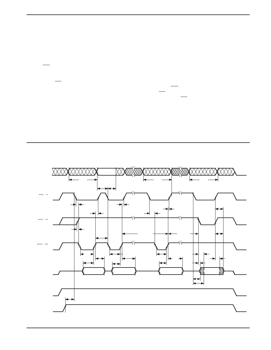
Figure 6. A.C. Timing for Programming Operation
Erase Mode
During the first Write cycle, the command 20H is written
into the command register. In order to commence the
erase operation, the identical command of 20H has to be
written again into the register. This two-step process
ensures against accidental erasure of the memory con-
tents. The final erase cycle will be stopped at the rising
edge of WE, at which time the Erase Verify command
(A0H) is sent to the command register. During this cycle,
the address to be verified is sent to the address bus and
latched when WE goes low. An integrated stop timer
allows for automatic timing control over this operation,
eliminating the need for a maximum erase timing speci-
fication. Refer to AC Characteristics (Program/Erase)
for specific timing parameters.
Erase-Verify Mode
The Erase-verify operation is performed on every byte
after each erase pulse to verify that the bits have been
erased.
Programming Mode
The programming operation is initiated using the pro-
gramming algorithm of Figure 7. During the first write
cycle, the command 40H is written into the command
register. During the second write cycle, the address of
the memory location to be programmed is latched on the
falling edge of WE, while the data is latched on the rising
edge of WE. The program operation terminates with the
next rising edge of WE. An integrated stop timer allows
for automatic timing control over this operation, eliminat-
ing the need for a maximum program timing specifica-
tion. Refer to AC Characteristics (Program/Erase) for
specific timing parameters.
相关PDF资料 |
PDF描述 |
|---|---|
| CAT28F010H14I-90TE13 | 128K X 8 FLASH 12V PROM, 90 ns, PDSO32 |
| CAT28F010TI-12TE13 | 128K X 8 FLASH 12V PROM, 120 ns, PDSO32 |
| CAT28F010TR-12TE7 | 128K X 8 FLASH 12V PROM, 120 ns, PDSO32 |
| CAT34WC02GYI-TE13REV-C | 256 X 8 I2C/2-WIRE SERIAL EEPROM, PDSO8 |
| CAT505J | SPECIALTY ANALOG CIRCUIT, PDSO20 |
相关代理商/技术参数 |
参数描述 |
|---|---|
| CAT28F010HRI-90T | 功能描述:闪存 1 Megabit Boot Block 闪存 Memory RoHS:否 制造商:ON Semiconductor 数据总线宽度:1 bit 存储类型:Flash 存储容量:2 MB 结构:256 K x 8 定时类型: 接口类型:SPI 访问时间: 电源电压-最大:3.6 V 电源电压-最小:2.3 V 最大工作电流:15 mA 工作温度:- 40 C to + 85 C 安装风格:SMD/SMT 封装 / 箱体: 封装:Reel |
| CAT28F010L12 | 功能描述:闪存 (128x8) 1M 120ns RoHS:否 制造商:ON Semiconductor 数据总线宽度:1 bit 存储类型:Flash 存储容量:2 MB 结构:256 K x 8 定时类型: 接口类型:SPI 访问时间: 电源电压-最大:3.6 V 电源电压-最小:2.3 V 最大工作电流:15 mA 工作温度:- 40 C to + 85 C 安装风格:SMD/SMT 封装 / 箱体: 封装:Reel |
| CAT28F010L-12 | 制造商:ON Semiconductor 功能描述:Flash Memory IC |
| CAT28F010L90 | 功能描述:闪存 (128x8) 1M 90ns RoHS:否 制造商:ON Semiconductor 数据总线宽度:1 bit 存储类型:Flash 存储容量:2 MB 结构:256 K x 8 定时类型: 接口类型:SPI 访问时间: 电源电压-最大:3.6 V 电源电压-最小:2.3 V 最大工作电流:15 mA 工作温度:- 40 C to + 85 C 安装风格:SMD/SMT 封装 / 箱体: 封装:Reel |
| CAT28F010L-90 | 制造商:Rochester Electronics LLC 功能描述: |
发布紧急采购,3分钟左右您将得到回复。