- 您现在的位置:买卖IC网 > PDF目录16993 > CDB5526 (Cirrus Logic Inc)EVAL BOARD FOR CS5526 PDF资料下载
参数资料
| 型号: | CDB5526 |
| 厂商: | Cirrus Logic Inc |
| 文件页数: | 16/30页 |
| 文件大小: | 0K |
| 描述: | EVAL BOARD FOR CS5526 |
| 标准包装: | 1 |
| ADC 的数量: | 1 |
| 位数: | 20 |
| 采样率(每秒): | 606 |
| 数据接口: | 串行 |
| 输入范围: | ±2.5 V |
| 在以下条件下的电源(标准): | 9.4mW @ 15SPS,5 V |
| 工作温度: | -40°C ~ 85°C |
| 已用 IC / 零件: | CS5526 |
| 已供物品: | 板,CD |
| 相关产品: | CS5526-BSZR-ND - IC ADC 20BIT W/4BIT LATCH 20SSOP 598-1108-5-ND - IC ADC 20BIT W/4BIT LATCH 20SSOP |
| 其它名称: | 598-1014 |
第1页第2页第3页第4页第5页第6页第7页第8页第9页第10页第11页第12页第13页第14页第15页当前第16页第17页第18页第19页第20页第21页第22页第23页第24页第25页第26页第27页第28页第29页第30页
CS5525 CS5526
DS202F5
23
the conversion data bits can be completely erroneous.
The OD flag bit will be cleared to logic 0 when the
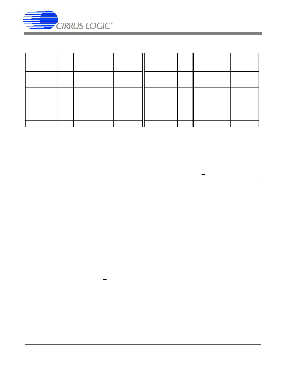
modulator becomes stable. Table 6 illustrates the out-
put coding for the CS5525/26.
Power Consumption
The CS5525/26 accommodate four power consump-
tion modes: normal, low power, standby, and sleep.
The normal mode, the default mode, is entered after a
power-on-reset and typically consumes 9.4 mW. The
low power mode is an alternate mode that reduces the
consumed power to 4.9 mW. It is entered by setting
bit D16 (the low power mode bit) in the configuration
register to logic 1. Since the converter’s noise perfor-
mance improves with increased power consumption,
slightly degraded noise or linearity performance
should be expected in the low power mode. The final
two modes are referred to as the power save modes.
They power down most of the analog portion of the
chips and stop filter convolutions. The power save
modes are entered whenever the PS/R bit and the CB
bit of the command word are set to logic 1. The par-
ticular power save mode entered depends on state of
bit D4 (the Power Save Select bit) in the configura-
tion register. If D4 is logic 0, the converters enters the
standby mode reducing the power consumption to
1.2mW. The standby mode leaves the oscillator and
the on-chip bias generator running. This allows the
converters to quickly return to the normal or low
power mode once the PS/R bit is set back to a logic 1.
If D4 in the configuration register and CB and PS/R
in the command word are set to logic 1, the sleep
mode is entered reducing the consumed power to less
than 500 W. Since the sleep mode disables the oscil-
lator, approximately a 500ms oscillator start-up delay
period is required before returning to the normal or
low power mode.
PCB Layout
The CS5525/26 should be placed entirely over an an-
alog ground plane with both the AGND and DGND
pins of the device connected to the analog plane.
Place the analog-digital plane split immediately adja-
cent to the digital portion of the chip.
The XIN pin represents a very high impedance when
used with a crystal, so care should be taken in routing
the trace from the crystal to the XIN pin to keep it as
short as possible. Stray capacitance between the CPD
pin and the XIN pin should be minimizedby keeping
the CPD pin trace away from XIN.
Note: VFS in the table equals the voltage between ground and full scale for any of the unipolar gain ranges, or the
voltage between
± full scale for any of the bipolar gain ranges. See text about error flags under overrange
conditions.
Unipolar Input
Voltage
Offset
Binary
Bipolar Input
Voltage
Two's
Complement
Unipolar Input
Voltage
Offset
Binary
Bipolar Input
Voltage
Two's
Complement
>(VFS-1.5 LSB)
FFFF
>(VFS-1.5 LSB)
7FFF
>(VFS-1.5 LSB) FFFFF
>(VFS-1.5 LSB)
7FFFF
VFS-1.5 LSB
FFFF
-----
FFFE
VFS-1.5 LSB
7FFF
-----
7FFE
VFS-1.5 LSB
FFFFF
-----
FFFFE
VFS-1.5 LSB
7FFFF
-----
7FFFE
VFS/2-0.5 LSB
8000
-----
7FFF
-0.5 LSB
0000
-----
FFFF
VFS/2-0.5 LSB
80000
-----
7FFFF
-0.5 LSB
00000
-----
FFFFF
+0.5 LSB
0001
-----
0000
-VFS+0.5 LSB
8001
-----
8000
+0.5 LSB
00001
-----
00000
-VFS+0.5 LSB
80001
-----
80000
<(+0.5 LSB)
0000
<(-VFS+0.5 LSB)
8000
<(+0.5 LSB)
00000
<(-VFS+0.5 LSB)
80000
Table 6. 5525/26 Output Coding
CS5525 16-Bit Output Coding
CS5526 20-Bit Output Coding
相关PDF资料 |
PDF描述 |
|---|---|
| 1025R-40K | COIL 6.8UH MOLDED UNSHIELDED |
| 222A111-4/86-0 | BOOT MOLDED |
| VI-J0Y-EX | CONVERTER MOD DC/DC 3.3V 49.5W |
| VE-J7V-EY | CONVERTER MOD DC/DC 5.8V 50W |
| 0150150623 | CABLE FLAT FLEX 23POS .3MM 6" |
相关代理商/技术参数 |
参数描述 |
|---|---|
| CDB5528 | 制造商:CIRRUS 制造商全称:Cirrus Logic 功能描述:Evaluation Board and Software |
| CDB5529 | 功能描述:EVAL BOARD FOR CS5529 RoHS:否 类别:编程器,开发系统 >> 评估板 - 模数转换器 (ADC) 系列:- 产品培训模块:Obsolescence Mitigation Program 标准包装:1 系列:- ADC 的数量:1 位数:12 采样率(每秒):94.4k 数据接口:USB 输入范围:±VREF/2 在以下条件下的电源(标准):- 工作温度:-40°C ~ 85°C 已用 IC / 零件:MAX11645 已供物品:板,软件 |
| CDB5530U | 功能描述:数据转换 IC 开发工具 Eval Bd 24-Bit 1-Ch Low-Noise ADC RoHS:否 制造商:Texas Instruments 产品:Demonstration Kits 类型:ADC 工具用于评估:ADS130E08 接口类型:SPI 工作电源电压:- 6 V to + 6 V |
| CDB5532U | 功能描述:数据转换 IC 开发工具 Eval Bd 24Bit ADC w/ Ultra Low-Noise USB RoHS:否 制造商:Texas Instruments 产品:Demonstration Kits 类型:ADC 工具用于评估:ADS130E08 接口类型:SPI 工作电源电压:- 6 V to + 6 V |
| CDB5534U | 功能描述:数据转换 IC 开发工具 Eval Bd 24Bit ADC w/ Ultra Low-Noise USB RoHS:否 制造商:Texas Instruments 产品:Demonstration Kits 类型:ADC 工具用于评估:ADS130E08 接口类型:SPI 工作电源电压:- 6 V to + 6 V |
发布紧急采购,3分钟左右您将得到回复。