参数资料
| 型号: | CDC2509BPWG4 |
| 厂商: | Texas Instruments |
| 文件页数: | 1/14页 |
| 文件大小: | 0K |
| 描述: | IC PLL CLOCK DVR 3.3V 24-TSSOP |
| 标准包装: | 60 |
| 类型: | PLL 时钟驱动器 |
| PLL: | 带旁路 |
| 输入: | LVTTL |
| 输出: | LVTTL |
| 电路数: | 1 |
| 比率 - 输入:输出: | 1:9 |
| 差分 - 输入:输出: | 无/无 |
| 频率 - 最大: | 125MHz |
| 除法器/乘法器: | 无/无 |
| 电源电压: | 3 V ~ 3.6 V |
| 工作温度: | 0°C ~ 70°C |
| 安装类型: | 表面贴装 |
| 封装/外壳: | 24-TSSOP(0.173",4.40mm 宽) |
| 供应商设备封装: | 24-TSSOP |
| 包装: | 管件 |
CDC2509B
3.3V PHASELOCK LOOP CLOCK DRIVER
SCAS613C SEPTEMBER 1998 REVISED DECEMBER 2004
1
POST OFFICE BOX 655303
DALLAS, TEXAS 75265
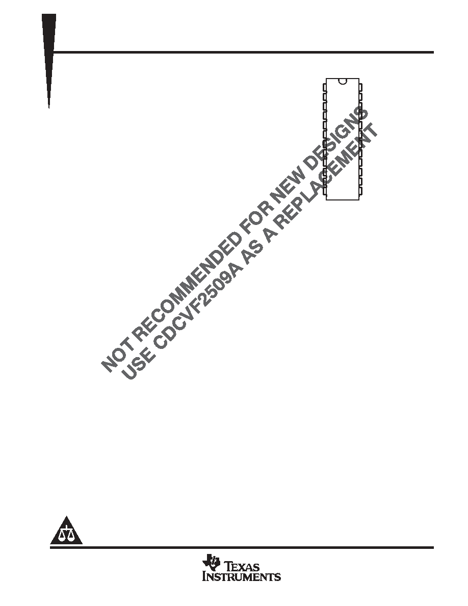
D Use CDCVF2509A as a Replacement for
this Device
D Designed to Meet PC SDRAM Registered
DIMM Specification
D Spread Spectrum Clock Compatible
D Operating Frequency 25 MHz to 125 MHz
D Phase Error Time Minus Jitter at 66 MHz to
100 MHz Is
±150 ps
D Jitter (peak peak) at 66 MHz to 100 MHz Is
±80 ps
D Jitter (cycle cycle) at 66 MHz to 100 MHz
Is |100 ps|
D Available in Plastic 24-Pin TSSOP
D Phase-Lock Loop Clock Distribution for
Synchronous DRAM Applications
D Distributes One Clock Input to One Bank of
Five and One Bank of Four Outputs
D Separate Output Enable for Each Output
Bank
D External Feedback (FBIN) Terminal Is Used
to Synchronize the Outputs to the Clock
Input
D On-Chip Series Damping Resistors
D No External RC Network Required
D Operates at 3.3 V
description
The CDC2509B is a high-performance, low-skew, low-jitter, phase-lock loop (PLL) clock drivers. They use a PLL
to precisely align, in both frequency and phase, the feedback (FBOUT) output to the clock (CLK) input signal.
They are specifically designed for use with synchronous DRAMs. The CDC2509B operates at 3.3-V VCC. They
also provide integrated series-damping resistors that make it ideal for driving point-to-point loads.
One bank of five outputs and one bank of four outputs provide nine low-skew, low-jitter copies of CLK. Output
signal duty cycles are adjusted to 50%, independent of the duty cycle at CLK. Each bank of outputs is enabled
or disabled separately via the control (1G and 2G) inputs. When the G inputs are high, the outputs switch in
phase and frequency with CLK; when the G inputs are low, the outputs are disabled to the logic-low state.
Unlike many products containing PLLs, the CDC2509B does not require external RC networks. The loop filter
for the PLL is included on-chip, minimizing component count, board space, and cost.
Because it is based on PLL circuitry, the CDC2509B requires a stabilization time to achieve phase lock of the
feedback signal to the reference signal. This stabilization time is required, following power up and application
of a fixed-frequency, fixed-phase signal at CLK, and following any changes to the PLL reference or feedback
signals. The PLL can be bypassed for test purposes by strapping AVCC to ground.
PRODUCTION DATA information is current as of publication date.
Products conform to specifications per the terms of Texas Instruments
standard warranty. Production processing does not necessarily include
testing of all parameters.
Copyright
2001 2004, Texas Instruments Incorporated
Please be aware that an important notice concerning availability, standard warranty, and use in critical applications of
Texas Instruments semiconductor products and disclaimers thereto appears at the end of this data sheet.
CLK
AVCC
VCC
2Y0
2Y1
GND
2Y2
2Y3
VCC
2G
FBIN
1
2
3
4
5
6
7
8
9
10
11
12
AGND
VCC
1Y0
1Y1
1Y2
GND
1Y3
1Y4
VCC
1G
FBOUT
24
23
22
21
20
19
18
17
16
15
14
13
PW PACKAGE
(TOP VIEW)
相关PDF资料 |
PDF描述 |
|---|---|
| V375A54T600B3 | CONVERTER MOD DC/DC 54V 600W |
| X9258US24IT2 | IC DGTL POT QUAD 100K 24SOIC |
| X9258US24IT1 | IC DGTL POT QUAD 100K 24SOIC |
| V375A54T600B2 | CONVERTER MOD DC/DC 54V 600W |
| MS27497T16B6S | CONN RCPT 6POS WALL MNT W/SCKT |
相关代理商/技术参数 |
参数描述 |
|---|---|
| CDC2509BPWLE | 制造商:未知厂家 制造商全称:未知厂家 功能描述:Nine Distributed-Output Clock Driver |
| CDC2509BPWR | 功能描述:时钟驱动器及分配 3.3V Clock RoHS:否 制造商:Micrel 乘法/除法因子:1:4 输出类型:Differential 最大输出频率:4.2 GHz 电源电压-最大: 电源电压-最小:5 V 最大工作温度:+ 85 C 封装 / 箱体:SOIC-8 封装:Reel |
| CDC2509BPWRG4 | 功能描述:时钟驱动器及分配 3.3V Clock RoHS:否 制造商:Micrel 乘法/除法因子:1:4 输出类型:Differential 最大输出频率:4.2 GHz 电源电压-最大: 电源电压-最小:5 V 最大工作温度:+ 85 C 封装 / 箱体:SOIC-8 封装:Reel |
| CDC2509BSTE-E | 功能描述:IC 3.3V PLL CLOCK DVR 24TSSOP RoHS:是 类别:集成电路 (IC) >> 时钟/计时 - 时钟发生器,PLL,频率合成器 系列:- 标准包装:2,000 系列:- 类型:PLL 时钟发生器 PLL:带旁路 输入:LVCMOS,LVPECL 输出:LVCMOS 电路数:1 比率 - 输入:输出:2:11 差分 - 输入:输出:是/无 频率 - 最大:240MHz 除法器/乘法器:是/无 电源电压:3.135 V ~ 3.465 V 工作温度:0°C ~ 70°C 安装类型:表面贴装 封装/外壳:32-LQFP 供应商设备封装:32-TQFP(7x7) 包装:带卷 (TR) |
| CDC2509C | 制造商:TI 制造商全称:Texas Instruments 功能描述:3.3-V PHASE-LOCK LOOP CLOCK DRIVER |
发布紧急采购,3分钟左右您将得到回复。