参数资料
| 型号: | CDC2509BPWG4 |
| 厂商: | Texas Instruments |
| 文件页数: | 10/14页 |
| 文件大小: | 0K |
| 描述: | IC PLL CLOCK DVR 3.3V 24-TSSOP |
| 标准包装: | 60 |
| 类型: | PLL 时钟驱动器 |
| PLL: | 带旁路 |
| 输入: | LVTTL |
| 输出: | LVTTL |
| 电路数: | 1 |
| 比率 - 输入:输出: | 1:9 |
| 差分 - 输入:输出: | 无/无 |
| 频率 - 最大: | 125MHz |
| 除法器/乘法器: | 无/无 |
| 电源电压: | 3 V ~ 3.6 V |
| 工作温度: | 0°C ~ 70°C |
| 安装类型: | 表面贴装 |
| 封装/外壳: | 24-TSSOP(0.173",4.40mm 宽) |
| 供应商设备封装: | 24-TSSOP |
| 包装: | 管件 |
CDC2509B
3.3V PHASELOCK LOOP CLOCK DRIVER
SCAS613C SEPTEMBER 1998 REVISED DECEMBER 2004
5
POST OFFICE BOX 655303
DALLAS, TEXAS 75265
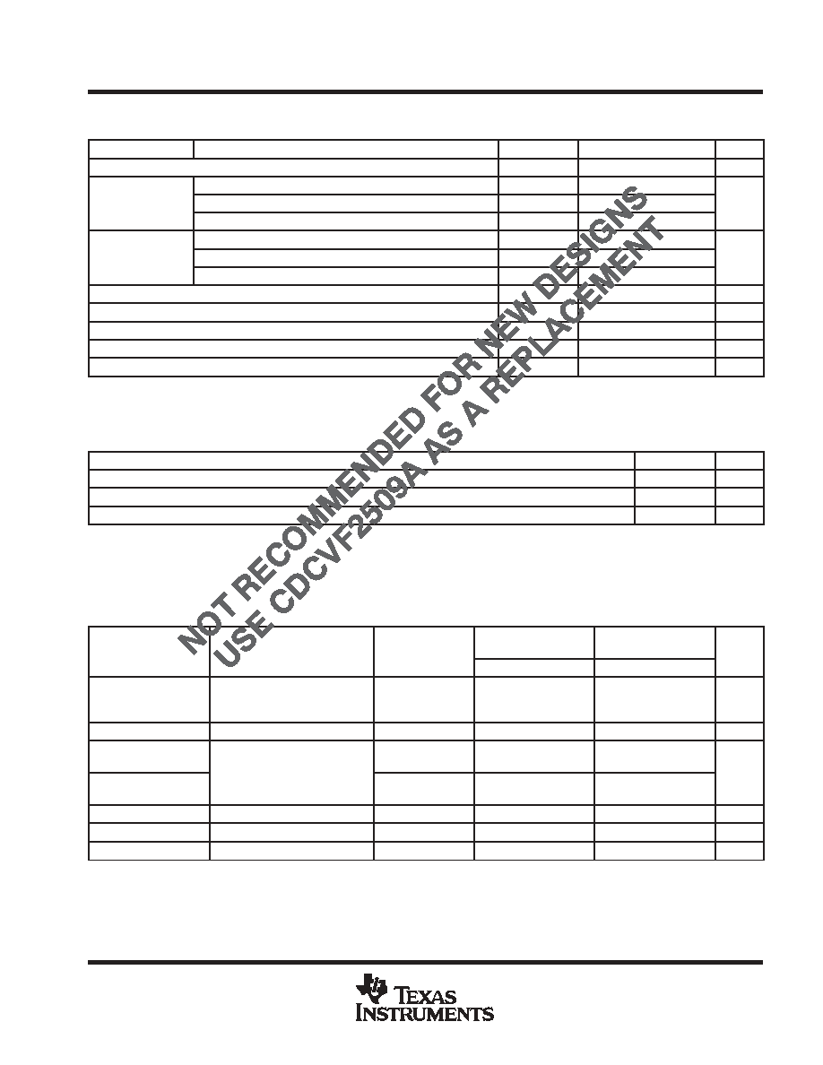
electrical characteristics over recommended operating free-air temperature range (unless
otherwise noted)
PARAMETER
TEST CONDITIONS
VCC, AVCC
MIN
TYP
MAX
UNIT
VIK
II = 18 mA
3 V
1.2
V
IOH = 100 A
MIN to MAX
VCC0.2
VOH
IOH = 12 mA
3 V
2.1
V
VOH
IOH = 6 mA
3 V
2.4
V
IOL = 100 A
MIN to MAX
0.2
VOL
IOL = 12 mA
3 V
0.8
V
VOL
IOL = 6 mA
3 V
0.55
V
II
VI = VCC or GND
3.6 V
±5
A
ICC
VI = VCC or GND,
IO = 0, Outputs: low or high
3.6 V
10
A
ICC
One input at VCC 0.6 V,
Other inputs at VCC or GND
3.3 V to 3.6 V
500
A
Ci
VI = VCC or GND
3.3 V
4
pF
Co
VO = VCC or GND
3.3 V
6
pF
For conditions shown as MIN or MAX, use the appropriate value specified under recommended operating conditions.
For ICC of AVCC, and ICC vs Frequency (see Figures 7 and 8).
timing requirements over recommended ranges of supply voltage and operating free-air
temperature
MIN
MAX
UNIT
fclk
Clock frequency
25
125
MHz
Input clock duty cycle
40%
60%
Stabilization time§
1
ms
§ Time required for the integrated PLL circuit to obtain phase lock of its feedback signal to its reference signal. For phase lock to be obtained, a
fixed-frequency, fixed-phase reference signal must be present at CLK. Until phase lock is obtained, the specifications for propagation delay, skew,
and jitter parameters given in the switching characteristics table are not applicable. This parameter does not apply for input modulation under
SSC application.
switching characteristics over recommended ranges of supply voltage and operating free-air
temperature, CL = 30 pF (see Note 6 and Figures 1 and 2)
PARAMETER
FROM
(INPUT)/CONDITION
TO
(OUTPUT)
VCC, AVCC = 3.3 V
± 0.165 V
VCC, AVCC = 3.3 V
± 0.3 V
UNIT
PARAMETER
(INPUT)/CONDITION
(OUTPUT)
MIN
TYP
MAX
MIN
TYP
MAX
UNIT
tphase error, jitter
(see Notes 7 and 8,
Figures 3, 4, and 5)
CLKIN
↑ = 66 MHz to100 MHz
FBIN
↑
150
200
ps
tsk(o)#
Any Y or FBOUT
200
ps
Jitter(pk-pk)
(see Figure 6)
CLKIN = 66 MHz to 100 MHz
Any Y or FBOUT
80
ps
Jitter(cycle-cycle)
(see Figure 6)
CLKIN = 66 MHz to 100 MHz
Any Y or FBOUT
|100|
ps
Duty cycle
F(CLKIN > 60 MHz)
Any Y or FBOUT
45%
55%
tr
Any Y or FBOUT
1.3
1.9
0.8
2.1
ns
tf
Any Y or FBOUT
1.7
2.5
1.2
2.7
ns
These parameters are not production tested.
# The tsk(o) specification is only valid for equal loading of all outputs.
NOTES:
6. The specifications for parameters in this table are applicable only after any appropriate stabilization time has elapsed.
7. This is considered as static phase error.
8. Phase error does not include jitter. The total phase error is 230 ps to 230 ps for the 5% VCC range.
相关PDF资料 |
PDF描述 |
|---|---|
| V375A54T600B3 | CONVERTER MOD DC/DC 54V 600W |
| X9258US24IT2 | IC DGTL POT QUAD 100K 24SOIC |
| X9258US24IT1 | IC DGTL POT QUAD 100K 24SOIC |
| V375A54T600B2 | CONVERTER MOD DC/DC 54V 600W |
| MS27497T16B6S | CONN RCPT 6POS WALL MNT W/SCKT |
相关代理商/技术参数 |
参数描述 |
|---|---|
| CDC2509BPWLE | 制造商:未知厂家 制造商全称:未知厂家 功能描述:Nine Distributed-Output Clock Driver |
| CDC2509BPWR | 功能描述:时钟驱动器及分配 3.3V Clock RoHS:否 制造商:Micrel 乘法/除法因子:1:4 输出类型:Differential 最大输出频率:4.2 GHz 电源电压-最大: 电源电压-最小:5 V 最大工作温度:+ 85 C 封装 / 箱体:SOIC-8 封装:Reel |
| CDC2509BPWRG4 | 功能描述:时钟驱动器及分配 3.3V Clock RoHS:否 制造商:Micrel 乘法/除法因子:1:4 输出类型:Differential 最大输出频率:4.2 GHz 电源电压-最大: 电源电压-最小:5 V 最大工作温度:+ 85 C 封装 / 箱体:SOIC-8 封装:Reel |
| CDC2509BSTE-E | 功能描述:IC 3.3V PLL CLOCK DVR 24TSSOP RoHS:是 类别:集成电路 (IC) >> 时钟/计时 - 时钟发生器,PLL,频率合成器 系列:- 标准包装:2,000 系列:- 类型:PLL 时钟发生器 PLL:带旁路 输入:LVCMOS,LVPECL 输出:LVCMOS 电路数:1 比率 - 输入:输出:2:11 差分 - 输入:输出:是/无 频率 - 最大:240MHz 除法器/乘法器:是/无 电源电压:3.135 V ~ 3.465 V 工作温度:0°C ~ 70°C 安装类型:表面贴装 封装/外壳:32-LQFP 供应商设备封装:32-TQFP(7x7) 包装:带卷 (TR) |
| CDC2509C | 制造商:TI 制造商全称:Texas Instruments 功能描述:3.3-V PHASE-LOCK LOOP CLOCK DRIVER |
发布紧急采购,3分钟左右您将得到回复。