- 您现在的位置:买卖IC网 > PDF目录2066 > CDCLVP2104RHDR (Texas Instruments)IC CLOCK BUFFER 2:8 2GHZ 28-VQFN PDF资料下载
参数资料
| 型号: | CDCLVP2104RHDR |
| 厂商: | Texas Instruments |
| 文件页数: | 1/22页 |
| 文件大小: | 0K |
| 描述: | IC CLOCK BUFFER 2:8 2GHZ 28-VQFN |
| 标准包装: | 3,000 |
| 类型: | 扇出缓冲器(分配) |
| 电路数: | 2 |
| 比率 - 输入:输出: | 2:8 |
| 差分 - 输入:输出: | 是/是 |
| 输入: | LVCMOS,LVDS,LVPECL,LVTTL |
| 输出: | LVPECL |
| 频率 - 最大: | 2GHz |
| 电源电压: | 2.375 V ~ 3.6 V |
| 工作温度: | -40°C ~ 85°C |
| 安装类型: | 表面贴装 |
| 封装/外壳: | 28-VFQFN 裸露焊盘 |
| 供应商设备封装: | 28-VQFN-EP(5x5) |
| 包装: | 带卷 (TR) |
LVPECL
4
2
Reference
Generator
GND
OUTP[7...4]
OUTN[7...4]
LVPECL
4
OUTP[3...0]
OUTN[3...0]
V
AC_REF[1, 0]
V
CC
V
CC
V
CC
INP0
INN0
INP1
INN1
CDCLVP2104
SCAS889A
– OCTOBER 2009 – REVISED AUGUST 2011
Eight LVPECL Output,
High-Performance Clock Buffer
Check for Samples: CDCLVP2104
1
FEATURES
DESCRIPTION
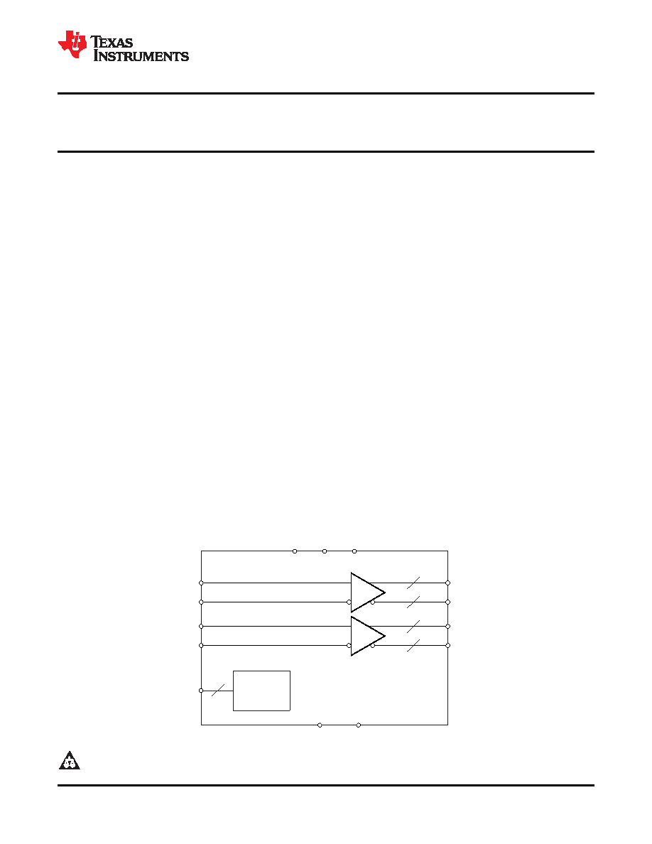
The CDCLVP2104 is a highly versatile, low additive
2
Dual 1:4 Differential Buffer
jitter buffer that can generate eight copies of LVPECL
Two Clock Inputs
clock outputs from two LVPECL, LVDS, or LVCMOS
Universal Inputs Can Accept LVPECL, LVDS,
inputs for a variety of communication applications. It
LVCMOS/LVTTL
has a maximum clock frequency up to 2 GHz. Each
buffer block consists of one input that feeds two
Eight LVPECL Outputs
LVPECL
outputs.
The
overall
additive
jitter
Maximum Clock Frequency: 2 GHz
performance is less than 0.1 ps, RMS from 10 kHz to
Maximum Core Current Consumption: 78 mA
20 MHz, and overall output skew is as low as 15 ps,
making the device a perfect choice for use in
Very Low Additive Jitter:
<100 fs,rms in 10-kHz
demanding applications.
to 20-MHz Offset Range
The CDCLVP2104 clock buffer distributes two clock
2.375 V to 3.6 V Device Power Supply
inputs (IN0, IN1) to eight pairs of differential LVPECL
Maximum Propagation Delay: 450 ps
clock outputs (OUT0, OUT7) with minimum skew for
Maximum 15 ps Within Bank Output Skew
clock distribution. Each buffer block consists of one
LVPECL Reference Voltage, VAC_REF, Available
input that feeds two LVPECL clock outputs. The
inputs can be LVPECL, LVDS, or LVCMOS/LVTTL.
for Capacitive-Coupled Inputs
Industrial Temperature Range:
–40°C to +85°C
The CDCLVP2104 is specifically designed for driving
50-
transmission lines. When driving the inputs in
Available in 5-mm
× 5-mm QFN-28 (RHD)
single-ended
mode,
the
LVPECL
bias
voltage
Package
(VAC_REF) should be applied to the unused negative
ESD Protection Exceeds 2 kV (HBM)
input pin. However, for high-speed performance up to
2 GHz, differential mode is strongly recommended.
APPLICATIONS
The CDCLVP2104 is characterized for operation
Wireless Communications
from
–40°C to +85°C and is available in a QFN-28,
Telecommunications/Networking
5-mm
× 5-mm package.
Medical Imaging
Test and Measurement Equipment
1
Please be aware that an important notice concerning availability, standard warranty, and use in critical applications of Texas
Instruments semiconductor products and disclaimers thereto appears at the end of this data sheet.
2
All trademarks are the property of their respective owners.
PRODUCTION DATA information is current as of publication date.
Copyright
2009–2011, Texas Instruments Incorporated
Products conform to specifications per the terms of the Texas
Instruments standard warranty. Production processing does not
necessarily include testing of all parameters.
相关PDF资料 |
PDF描述 |
|---|---|
| CMP04FS | IC COMPARATOR QUAD LP 14-SOIC |
| CMP402GS-REEL | IC COMPARATOR LV 65NS 16-SOIC |
| CS3308-CQZ | IC ANLG VOL CTRL 8CH DGTL 48LQFP |
| CS3310-KSZR | IC DGTL VOL CTRL 2CH 16-SOIC |
| CS3318-CQZR | IC ANLG VOL CTRL 8CH 48-LQFP |
相关代理商/技术参数 |
参数描述 |
|---|---|
| CDCLVP2104RHDT | 功能描述:时钟缓冲器 Low Jtr Dual 1:4 Uni-to-LVPECL Bfr RoHS:否 制造商:Texas Instruments 输出端数量:5 最大输入频率:40 MHz 传播延迟(最大值): 电源电压-最大:3.45 V 电源电压-最小:2.375 V 最大功率耗散: 最大工作温度:+ 85 C 最小工作温度:- 40 C 封装 / 箱体:LLP-24 封装:Reel |
| CDCLVP2106 | 制造商:TI 制造商全称:Texas Instruments 功能描述:12 LVPECL Output, High-Performance Clock Buffer |
| CDCLVP2106EVM | 功能描述:时钟和定时器开发工具 CDCLVP2106 Eval Mod RoHS:否 制造商:Texas Instruments 产品:Evaluation Modules 类型:Clock Conditioners 工具用于评估:LMK04100B 频率:122.8 MHz 工作电源电压:3.3 V |
| CDCLVP2106RHAR | 功能描述:时钟缓冲器 Low Jitter Dual 1:6 Univ-to-LVPECL Bfr RoHS:否 制造商:Texas Instruments 输出端数量:5 最大输入频率:40 MHz 传播延迟(最大值): 电源电压-最大:3.45 V 电源电压-最小:2.375 V 最大功率耗散: 最大工作温度:+ 85 C 最小工作温度:- 40 C 封装 / 箱体:LLP-24 封装:Reel |
| CDCLVP2106RHAT | 功能描述:时钟缓冲器 Low Jitter Dual 1:6 Univ-to-LVPECL Bfr RoHS:否 制造商:Texas Instruments 输出端数量:5 最大输入频率:40 MHz 传播延迟(最大值): 电源电压-最大:3.45 V 电源电压-最小:2.375 V 最大功率耗散: 最大工作温度:+ 85 C 最小工作温度:- 40 C 封装 / 箱体:LLP-24 封装:Reel |
发布紧急采购,3分钟左右您将得到回复。