- 您现在的位置:买卖IC网 > PDF目录2066 > CDCLVP2104RHDR (Texas Instruments)IC CLOCK BUFFER 2:8 2GHZ 28-VQFN PDF资料下载
参数资料
| 型号: | CDCLVP2104RHDR |
| 厂商: | Texas Instruments |
| 文件页数: | 3/22页 |
| 文件大小: | 0K |
| 描述: | IC CLOCK BUFFER 2:8 2GHZ 28-VQFN |
| 标准包装: | 3,000 |
| 类型: | 扇出缓冲器(分配) |
| 电路数: | 2 |
| 比率 - 输入:输出: | 2:8 |
| 差分 - 输入:输出: | 是/是 |
| 输入: | LVCMOS,LVDS,LVPECL,LVTTL |
| 输出: | LVPECL |
| 频率 - 最大: | 2GHz |
| 电源电压: | 2.375 V ~ 3.6 V |
| 工作温度: | -40°C ~ 85°C |
| 安装类型: | 表面贴装 |
| 封装/外壳: | 28-VFQFN 裸露焊盘 |
| 供应商设备封装: | 28-VQFN-EP(5x5) |
| 包装: | 带卷 (TR) |
3,0mm(min)
0,75mm(typ)
0,33mm(typ)
SCAS889A
– OCTOBER 2009 – REVISED AUGUST 2011
APPLICATION INFORMATION
Thermal Management
Power consumption of the CDCLVP2104 can be high enough to require attention to thermal management. For
reliability and performance reasons, the die temperature should be limited to a maximum of +125
°C. That is, as
an estimate, ambient temperature (TA) plus device power consumption times θJA should not exceed +125°C.
The device package has an exposed pad that provides the primary heat removal path to the printed circuit board
(PCB). To maximize the heat dissipation from the package, a thermal landing pattern including multiple vias to a
ground plane must be incorporated into the PCB within the footprint of the package. The exposed pad must be
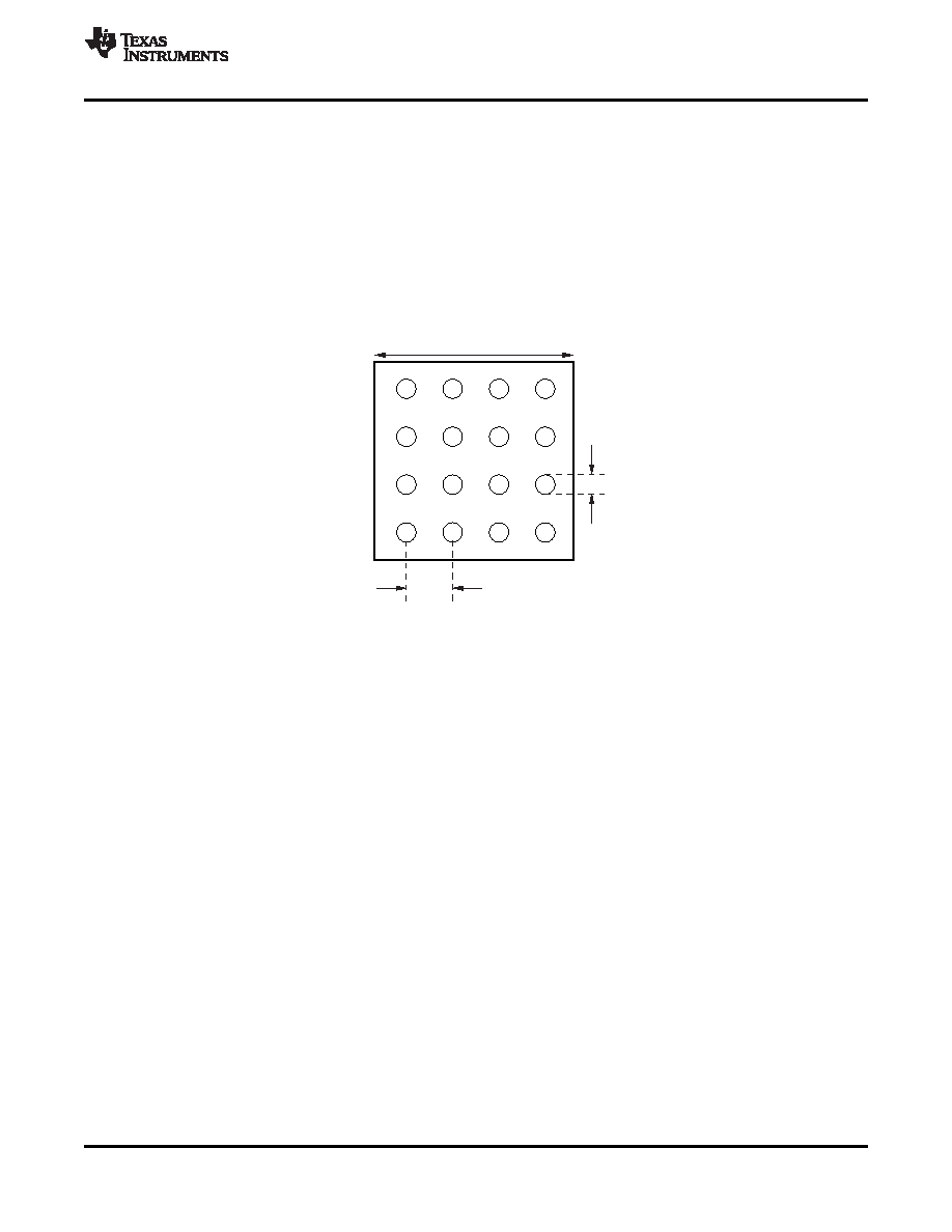
soldered down to ensure adequate heat conduction out of the package. Figure 12 shows a recommended land
and via pattern.
Figure 12. Recommended PCB Layout
Power-Supply Filtering
High-performance clock buffers are sensitive to noise on the power supply, which can dramatically increase the
additive jitter of the buffer. Thus, it is essential to reduce noise from the system power supply, especially when
jitter/phase noise is very critical to applications.
Filter capacitors are used to eliminate the low-frequency noise from the power supply, where the bypass
capacitors provide the very low impedance path for high-frequency noise and guard the power-supply system
against the induced fluctuations. These bypass capacitors also provide instantaneous current surges as required
by the device and should have low equivalent series resistance (ESR). To properly use the bypass capacitors,
they must be placed very close to the power-supply pins and laid out with short loops to minimize inductance. It
is recommended to add as many high-frequency (for example, 0.1-
μF) bypass capacitors as there are supply
pins in the package. It is recommended, but not required, to insert a ferrite bead between the board power supply
and the chip power supply that isolates the high-frequency switching noises generated by the clock driver; these
beads prevent the switching noise from leaking into the board supply. Choose an appropriate ferrite bead with
very low dc resistance because it is imperative to provide adequate isolation between the board supply and the
chip supply, as well as to maintain a voltage at the supply pins that is greater than the minimum voltage required
for proper operation.
Copyright
2009–2011, Texas Instruments Incorporated
11
Product Folder Link(s): CDCLVP2104
相关PDF资料 |
PDF描述 |
|---|---|
| CMP04FS | IC COMPARATOR QUAD LP 14-SOIC |
| CMP402GS-REEL | IC COMPARATOR LV 65NS 16-SOIC |
| CS3308-CQZ | IC ANLG VOL CTRL 8CH DGTL 48LQFP |
| CS3310-KSZR | IC DGTL VOL CTRL 2CH 16-SOIC |
| CS3318-CQZR | IC ANLG VOL CTRL 8CH 48-LQFP |
相关代理商/技术参数 |
参数描述 |
|---|---|
| CDCLVP2104RHDT | 功能描述:时钟缓冲器 Low Jtr Dual 1:4 Uni-to-LVPECL Bfr RoHS:否 制造商:Texas Instruments 输出端数量:5 最大输入频率:40 MHz 传播延迟(最大值): 电源电压-最大:3.45 V 电源电压-最小:2.375 V 最大功率耗散: 最大工作温度:+ 85 C 最小工作温度:- 40 C 封装 / 箱体:LLP-24 封装:Reel |
| CDCLVP2106 | 制造商:TI 制造商全称:Texas Instruments 功能描述:12 LVPECL Output, High-Performance Clock Buffer |
| CDCLVP2106EVM | 功能描述:时钟和定时器开发工具 CDCLVP2106 Eval Mod RoHS:否 制造商:Texas Instruments 产品:Evaluation Modules 类型:Clock Conditioners 工具用于评估:LMK04100B 频率:122.8 MHz 工作电源电压:3.3 V |
| CDCLVP2106RHAR | 功能描述:时钟缓冲器 Low Jitter Dual 1:6 Univ-to-LVPECL Bfr RoHS:否 制造商:Texas Instruments 输出端数量:5 最大输入频率:40 MHz 传播延迟(最大值): 电源电压-最大:3.45 V 电源电压-最小:2.375 V 最大功率耗散: 最大工作温度:+ 85 C 最小工作温度:- 40 C 封装 / 箱体:LLP-24 封装:Reel |
| CDCLVP2106RHAT | 功能描述:时钟缓冲器 Low Jitter Dual 1:6 Univ-to-LVPECL Bfr RoHS:否 制造商:Texas Instruments 输出端数量:5 最大输入频率:40 MHz 传播延迟(最大值): 电源电压-最大:3.45 V 电源电压-最小:2.375 V 最大功率耗散: 最大工作温度:+ 85 C 最小工作温度:- 40 C 封装 / 箱体:LLP-24 封装:Reel |
发布紧急采购,3分钟左右您将得到回复。