- 您现在的位置:买卖IC网 > PDF目录26498 > CDS-1401MM (MURATA POWER SOLUTIONS INC) PDF资料下载
参数资料
| 型号: | CDS-1401MM |
| 厂商: | MURATA POWER SOLUTIONS INC |
| 元件分类: | 取样保持放大器 |
| 中文描述: | SAMPLE AND HOLD AMPLIFIER, 0.35 us ACQUISITION TIME, CDIP24 |
| 封装: | CERAMIC, DDIP-24 |
| 文件页数: | 7/8页 |
| 文件大小: | 87K |
| 代理商: | CDS-1401MM |
7
CDS-1401
CALIBRATION PROCEDURE
Offset Adjust (Figure 5)
Offset and pedestal errors may be compensated for by
applying external voltages to pin 1 (OFFSET ADJUST V1) and/
or pin 9 (OFFSET ADJUST V2) using either voltage-output
DAC’s or potentiometers configured to appear as voltage
sources.
Offset and pedestal errors may also be compensated for by
applying external currents to pin 2 (OFFSET ADJUST I1) and/
or pin 10 (OFFSET ADJUST I2) by using either current-output
DAC’s or potentiometers configured to appear as current
sources.
1. Connect pin 8 (S/H2 SUMMING NODE) either directly to
pin 7 (S/H1 ROUT) or through a 200 Ohm potentiometer to
pin 6 (S/H1 OUT).
2. Tie pins 3 (ANALOG INPUT 1) and 4 (ANALOG INPUT 2)
to pin 5 (ANALOG GROUND).
3. Adjust OFFSET ADJUST V1 or OFFSET ADJUST I1 (while
S/H1 is in the hold mode) until pin 6 (S/H1 OUT) equals 0V.
4. Adjust OFFSET ADJUST V2 or OFFSET ADJUST I2 (while
S/H2 is in the hold mode) until pin 22 (VOUT) equals 0V.
5. To negate the effect of output droop on the offset-adjust
process, each S/H must be continually switched between its
sample and hold modes and adjusted so its output equals
zero immediately after going into the hold mode.
The sensitivity of the voltage offset adjustments is 100mV per
Volt. The sensitivity of the current offset adjustments is
1V per mA. Pins 1, 2, 9 and 10 should be left open (floating)
when not being used for offset adjustment.
Gross Offset Adjustment
For gross offset adjustments use pin 2 (OFFSET ADJUST I1)
and/or pin 10 (OFFSET ADJUST I2). All connections made to
pin 2 and pin 10 should be very short because these are very
sensitive points.
Sourcing 1mA into OFFSET ADJUST I1 will cause a –1V offset
change at pin 6 (S/H1 OUT). It will also cause a +1V offset
change at pin 22 (V OUT) if pin 7 (S/H1 ROUT) is connected to
pin 8 (S/H2 SUMMING NODE).
Sourcing 1mA into OFFSET ADJUST I2 will cause a –1V offset
change at pin 22 (V OUT).
Gain Matching Adjustment (Differential Gain)
between S/H1 and S/H2
The user can adjust the gain matching (differential gain)
between S/H1 and S/H2 by leaving pin 7 (S/H1 ROUT) floating
(open) and connecting a 200 Ohm potentiometer between pin
6 (S/H1 OUT) and pin 8 (S/H2 SUMMING NODE). Note, offset
adjustment should take place before gain matching
adjustment.
Apply a full-scale input to both pins 3 (ANALOG INPUT 1) and
4 (ANALOG INPUT 2). Adjust the 200 Ohm potentiometer
(with both S/H's in the sample mode) until pin 22 (V OUT) is
0V.
If gain matching adjustment is not required, leave pin 6 (S/H1
OUT) floating (open) and tie pin 7 (S/H1 ROUT) to pin 8 (S/H2
SUMMING NODE).
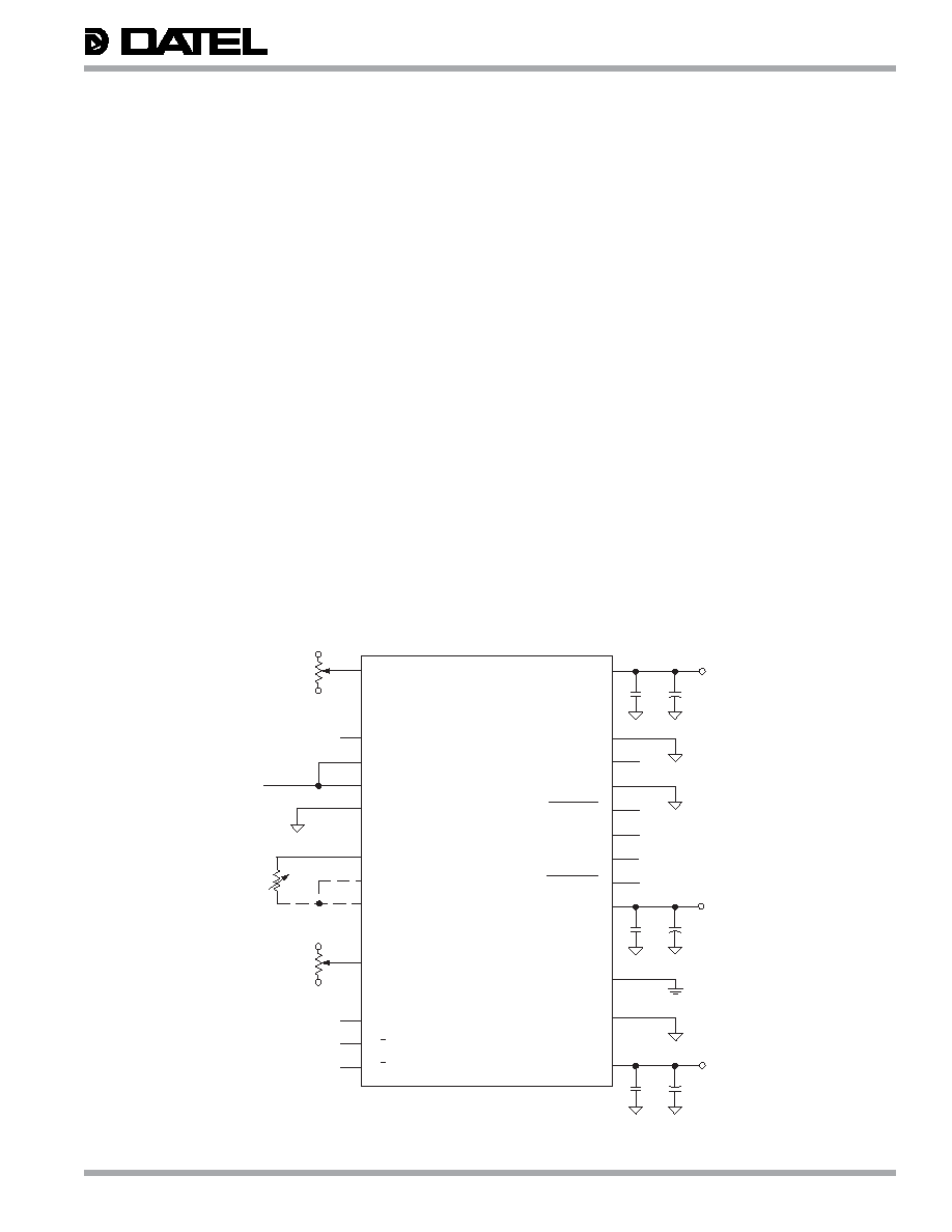
Figure 5. CDS-1401 Typical Connection Diagram
OFFSET ADJUST V1
1
+15V
–15V
OFFSET ADJUST I1
2
ANALOG INPUT 1
3
ANALOG INPUT 2
4
ANALOG GROUND
5
S/H1 OUT
6
S/H1 ROUT
7
S/H2 SUMMING NODE
8
OFFSET ADJUST V2
9
+15V
–15V
OFFSET ADJUST I2
10
S/H1 COMMAND
11
S/H2 COMMAND
12
200
0.1F
2.2F
+15V
+
0.1F
2.2F
+
–15V
0.1F
2.2F
+5V
+
24
23
22
21
20
19
18
17
16
15
14
13
ANALOG GROUND
V OUT
ANALOG GROUND
A/D CLOCK 2
A/D CLOCK 1
+5V DIGITAL SUPPLY
DIGITAL GROUND
ANALOG GROUND
–15V ANALOG SUPPLY
+15V ANALOG SUPPLY
CDS-1401
相关PDF资料 |
PDF描述 |
|---|---|
| CDS-1402MC | |
| CFUKF455KB4X-R0 | |
| CFUKF455KD1X-R0 | |
| CFULB455KB2A-B0 | |
| CFULB455KF4A-B0 | |
相关代理商/技术参数 |
参数描述 |
|---|---|
| CDS1402 | 制造商:未知厂家 制造商全称:未知厂家 功能描述:14-Bit, Very Fast Settling Correlated Double Sampling Circuit |
| CDS-1402 | 制造商:未知厂家 制造商全称:未知厂家 功能描述:14-Bit, Very Fast Settling Correlated Double Sampling Circuit |
| CDS-1402MC | 制造商:Murata Power Solutions 功能描述:Correlated Double Sampler (Cds) 24-Pin CDDIP |
| CDS-1402MM | 制造商:Murata Power Solutions 功能描述:Correlated Double Sampler (Cds) 24-Pin CDDIP |
| CDS14N | 功能描述:SOCKET,1/4" DRIVE,7MM,6PT 制造商:apex tool group 系列:* 零件状态:在售 标准包装:1 |
发布紧急采购,3分钟左右您将得到回复。