- 您现在的位置:买卖IC网 > PDF目录378798 > CDS-1402MC (Electronic Theatre Controls, Inc.) 14-Bit, Very Fast Settling Correlated Double Sampling Circuit PDF资料下载
参数资料
| 型号: | CDS-1402MC |
| 厂商: | Electronic Theatre Controls, Inc. |
| 英文描述: | 14-Bit, Very Fast Settling Correlated Double Sampling Circuit |
| 中文描述: | 14位,非常快速沉降相关双采样电路 |
| 文件页数: | 1/8页 |
| 文件大小: | 203K |
| 代理商: | CDS-1402MC |
FEATURES
Use with 10 to 14-bit A/D converters
5 Megapixels/second minimum throughput (14 bits)
±2.5V input/output ranges, Gain = –1
Low noise, 200μVrms
Two independent S/H amplifiers
Gain matching between S/H's
Offset adjustments for each S/H
Four external A/D control lines
Small package, 24-pin ceramic DDIP
Low power, 350mW
Low cost
GENERAL DESCRIPTION
The CDS-1402 is an application-specific, correlated double
sampling (CDS) circuit designed for electronic-imaging
applications that employ CCD's (charge coupled devices) as
their photodetector. The CDS-1402 has been optimized for
use in digital video applications that employ 10 to 14-bit A/D
converters. The low-noise CDS-1402 can accurately
determine each pixel's true video signal level by sequentially
sampling the pixel's offset signal and its video signal and
subtracting the two. The result is that the consequences of
residual charge, charge injection and low-frequency "kTC"
noise on the CCD's output floating capacitor are effectively
eliminated. The CDS-1402 can also be used as a dual
sample-hold amplifier in a data acquisition system.
The CDS-1402 contains two sample-hold amplifiers and
appropriate support/control circuitry. Features include
independent offset-adjust capability for each S/H,
adjustment for matching gain between the two S/H's,
CDS -1402
14-Bit, Very Fast Settling
Correlated Double Sampling Circuit
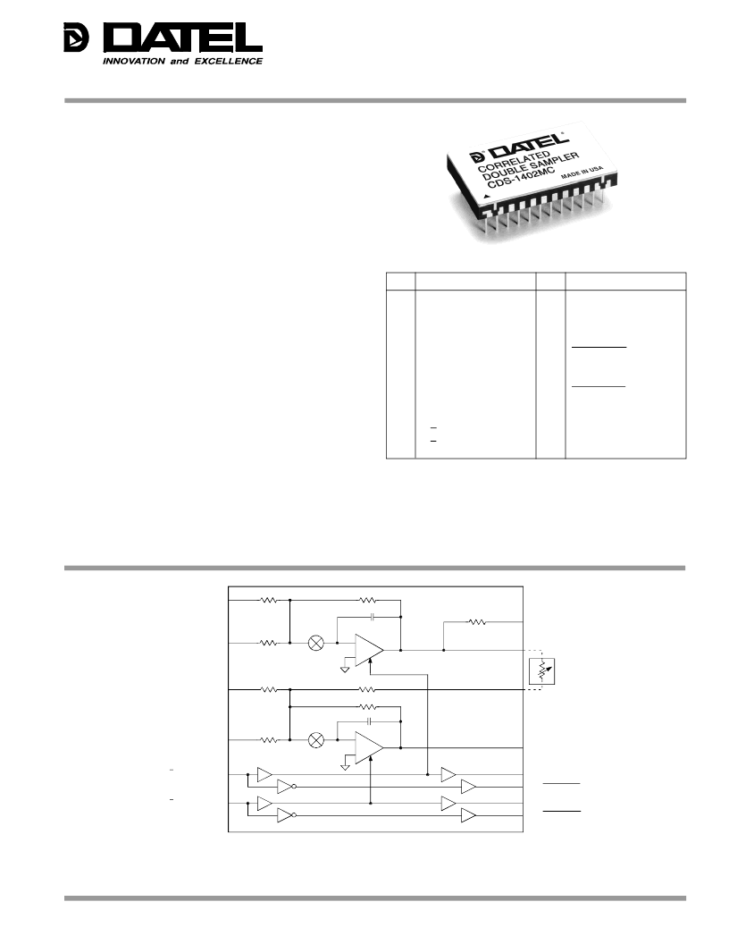
Figure 1. CDS-1402 Functional Block Diagram
(continued on page 3)
DATEL, Inc., 11 Cabot Boulevard, Mansfield, MA 02048-1151 (U.S.A.)
Tel: (508) 339-3000 Fax: (508) 339-6356
For immediate assistance: (800) 233-2765
S/H 2
+
OFFSET ADJUST V1 1
DO NOT CONNECT 2
ANALOG INPUT 1 3
OFFSET ADJUST V2 9
DO NOT CONNECT 10
ANALOG INPUT 2 4
S/H1 COMMAND 11
S/H2 COMMAND 12
5, 14, 21, 23
ANALOG GROUND
24
+5V ANALOG
SUPPLY
16
+5V DIGITAL
SUPPLY
15
DIGITAL
GROUND
7 S/H1 ROUT
8 S/H2
SUMMING NODE
22 V OUT
18 A/D CLOCK 1
6 S/H1 OUT
OPTIONAL
17 A/D CLOCK 1
19 A/D CLOCK 2
20 A/D CLOCK 2
100k
100k
450
500
13
–5V ANALOG
SUPPLY
–
S/H 1
+
–
500
500
500
50
C
H
C
H
1
2
3
4
5
6
7
8
9
10
11
12
OFFSET ADJUST V1
DO NOT CONNECT
ANALOG INPUT 1
ANALOG INPUT 2
ANALOG GROUND
S/H1 OUT
S/H1 ROUT
S/H2 SUMMING NODE
OFFSET ADJUST V2
DO NOT CONNECT
S/H1 COMMAND
S/H2 COMMAND
24
23
22
21
20
19
18
17
16
15
14
13
+5V ANALOG SUPPLY
ANALOG GROUND
V OUT
ANALOG GROUND
A/D CLOCK2
A/D CLOCK2
A/D CLOCK1
A/D CLOCK1
+5V DIGITAL SUPPLY
DIGITAL GROUND
ANALOG GROUND
–5V ANALOG SUPPLY
PIN
FUNCTION
PIN FUNCTION
and four control lines for triggering the A/D converter used in
conjunction with the CDS-1402. The CDS circuit's "ping-
pong" timing approach (the offset signal of the "n+1" pixel can
be acquired while the video output of the "nth" pixel is being
converted) guarantees a minimum throughput, in a 14-bit
application, of 5MHz. In other words, the true video signal
(minus offset) will be available
INPUT/OUTPUT CONNECTIONS
相关PDF资料 |
PDF描述 |
|---|---|
| CDS-1402 | 14-Bit, Very Fast Settling Correlated Double Sampling Circuit |
| CDS-1402MM | 14-Bit, Very Fast Settling Correlated Double Sampling Circuit |
| CDS15FD331J03 | Miniature Dipped, Mica Capacitors |
| CDS15CD180J03 | Miniature Dipped, Mica Capacitors |
| CDS15ED200J03 | Miniature Dipped, Mica Capacitors |
相关代理商/技术参数 |
参数描述 |
|---|---|
| CDS-1402MM | 制造商:Murata Power Solutions 功能描述:Correlated Double Sampler (Cds) 24-Pin CDDIP |
| CDS14N | 功能描述:SOCKET,1/4" DRIVE,7MM,6PT 制造商:apex tool group 系列:* 零件状态:在售 标准包装:1 |
| CDS15 | 功能描述:保险丝 CARTRIDGE D 15A RoHS:否 制造商:Littelfuse 产品:Surface Mount Fuses 电流额定值:0.5 A 电压额定值:600 V 保险丝类型:Fast Acting 保险丝大小/组:Nano 尺寸:12.1 mm L x 4.5 mm W 安装风格: 端接类型:SMD/SMT 系列:485 |
| CDS150 | 功能描述:保险丝 CNDIAN D-TYP 600V TD RoHS:否 制造商:Littelfuse 产品:Surface Mount Fuses 电流额定值:0.5 A 电压额定值:600 V 保险丝类型:Fast Acting 保险丝大小/组:Nano 尺寸:12.1 mm L x 4.5 mm W 安装风格: 端接类型:SMD/SMT 系列:485 |
| CDS-15118B | 功能描述:8 Ohm Magnetic Speaker 700mW 20Hz ~ 20kHz Top Rectangular 86dB 制造商:cui inc. 系列:CDS 零件状态:有效 类型:磁性 频率范围:20Hz ~ 20kHz 阻抗:8 欧姆 声压级:86dB 功率 - 额定值:700mW 功率 - 最大值:1W 端口位置:顶部 形状:矩形 材料 - 锥体:PET 材料 - 磁铁:Nd-Fe-B 端接:焊盘 大小/尺寸:15.00mm 长 x 11.00mm 宽 高度:3.10mm 标准包装:100 |
发布紧急采购,3分钟左右您将得到回复。