- 您现在的位置:买卖IC网 > PDF目录378445 > CH5101A (Electronic Theatre Controls, Inc.) CMOS Monochrome Digital Video Camera PDF资料下载
参数资料
| 型号: | CH5101A |
| 厂商: | Electronic Theatre Controls, Inc. |
| 英文描述: | CMOS Monochrome Digital Video Camera |
| 中文描述: | 单色的CMOS数码摄像机 |
| 文件页数: | 5/32页 |
| 文件大小: | 132K |
| 代理商: | CH5101A |
第1页第2页第3页第4页当前第5页第6页第7页第8页第9页第10页第11页第12页第13页第14页第15页第16页第17页第18页第19页第20页第21页第22页第23页第24页第25页第26页第27页第28页第29页第30页第31页第32页
CHRONTEL
CH5101A
201-0000-033 Rev 1.0, 6/2/99
5
HS*
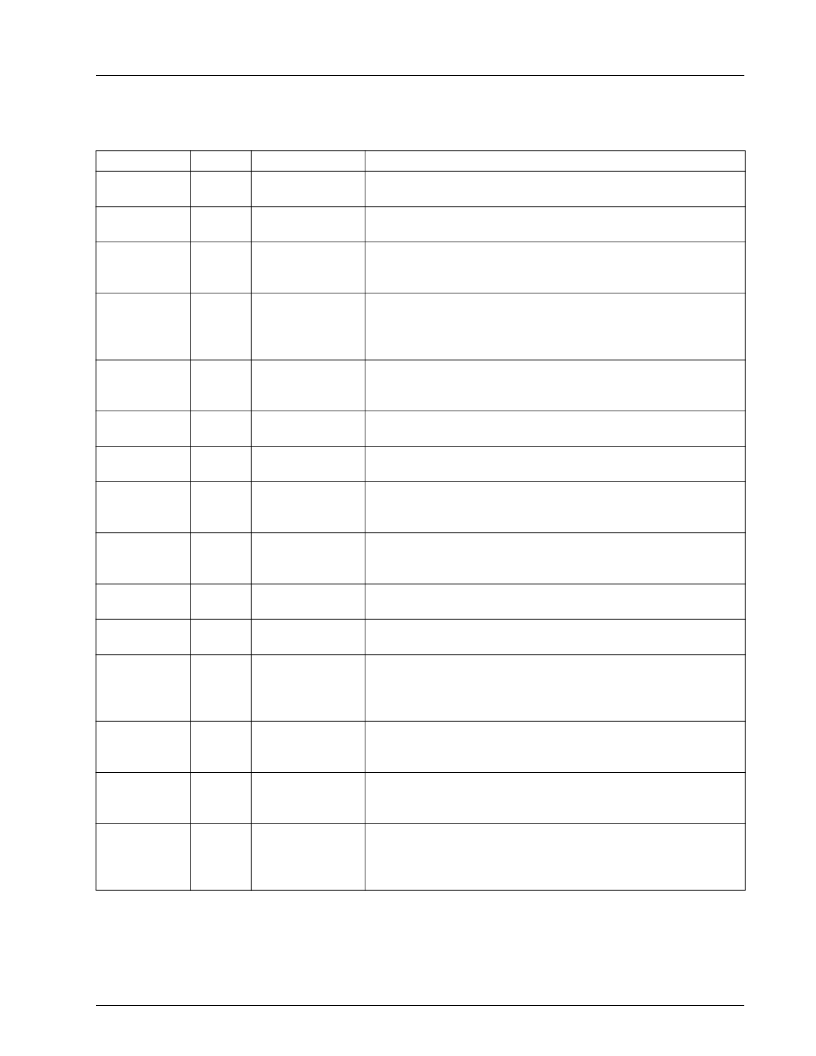
Table 1. Pin Descriptions Note:
Pin numbers in parenthesis ( ) are for 52 pin PQFP
Pin
Type
Out
Symbol
Description
21-14
(14-7)
Y[7:0]
Video Output
Provides the luminance data of the digital video output.
1,7,11,22,34,
(4,15,27,46,52)
Power
DVDD
Digital Supply Voltage
These pins supply the 5V power to the digital section of CH5101.
4,8,24,36,
(1, 17, 29, 49)
Power
DGND
Digital Ground
Provides the ground reference for the digital section of CH5101. These
pins MUST be connected to the system ground.
31-25
(24-18)
In
PUD[5:0]*
PUD[6]
Power Up Detect (internal pull-up)
These are inputs controlling the default value of IIC register bits
M0, ADDO, PD, ASW[3:0]. Attach 100K Ohms to DGND to pull low.
NOTE: PUD[5:0]* are logically inverted
23
(16)
Out
CLKOUT
Video Pixel Clock Output
This pin outputs a buffered clock signal which can be used to latch data
output by pins Y[7:0]
9
(2)
Out
VS*
Vertical Sync Output (active low)
Outputs a vertical sync pulse.
10
(3)
Out
Horizontal Sync Output (active low)
Outputs a horizontal sync pulse.
12
(5)
Out
OVR
Over Range
This pin is high when the A/D converter input is beyond the full scale
range of the A/D.
13
(6)
Out
HREF
Horizontal Reference
Active video timing signal. This output is high when active data is being
output from the device, and low otherwise.
6
(51)
In
SC
Serial Clock
IIC clock input pin.
5
(50)
In/Out
SD
Serial Data
IIC data input/output pin.
2
(47)
In
AS
Chip Address Select (internal pullup)
This pin selects the IIC address for the device.
AS = 1 Address = 100 0101
AS = 0 Address = 100 0110
3
(48)
In
RESET*
Chip Reset (active low, internal pullup)
Puts all registers into power-on default states. The state at pin SD must
be HIGH during reset for proper initialization.
38
(31)
In/Out
XO
Crystal Output
A 27 MHz (± 50 ppm, parallel resonance) crystal may be attached
between XO and XI/FIN.
39
(32)
In
XI/FIN
Crystal Input or External input
A 27 MHz (± 50 ppm, parallel resonance) crystal should be attached
between XO and XI/FIN. An external CMOS compatible clock can be
connected to XI/FIN as an alternative.
相关PDF资料 |
PDF描述 |
|---|---|
| CH5101A-L | CMOS Monochrome Digital Video Camera |
| CH7003B-T | Digital PC to TV Encoder |
| CH7003B | Digital PC to TV Encoder |
| CH7003B-V | Digital PC to TV Encoder |
| CH7006C | MODULE |
相关代理商/技术参数 |
参数描述 |
|---|---|
| CH5101A-L | 制造商:未知厂家 制造商全称:未知厂家 功能描述:CMOS Monochrome Digital Video Camera |
| CH5101A-Q | 制造商:未知厂家 制造商全称:未知厂家 功能描述:CMOS Monochrome Digital Video Camera |
| CH511H-30PT | 制造商:CHENMKO 制造商全称:Chenmko Enterprise Co. Ltd. 功能描述:SCHOTTKY BARRIER DIODE VOLTAGE 30 Volts CURRENT 1.0 Ampere |
| CH511H-40PT | 制造商:CHENMKO 制造商全称:Chenmko Enterprise Co. Ltd. 功能描述:SCHOTTKY BARRIER DIODE VOLTAGE 40 Volts CURRENT 1.0 Ampere |
| CH5125C6W | 制造商:Cooper Crouse-Hinds 功能描述: |
发布紧急采购,3分钟左右您将得到回复。