- 您现在的位置:买卖IC网 > PDF目录378829 > CH7009A-T (Electronic Theatre Controls, Inc.) Chrontel CH7009 DVI / TV Output Device PDF资料下载
参数资料
| 型号: | CH7009A-T |
| 厂商: | Electronic Theatre Controls, Inc. |
| 英文描述: | Chrontel CH7009 DVI / TV Output Device |
| 中文描述: | 昆泰CH7009和DVI / TV输出设备 |
| 文件页数: | 18/46页 |
| 文件大小: | 580K |
| 代理商: | CH7009A-T |
第1页第2页第3页第4页第5页第6页第7页第8页第9页第10页第11页第12页第13页第14页第15页第16页第17页当前第18页第19页第20页第21页第22页第23页第24页第25页第26页第27页第28页第29页第30页第31页第32页第33页第34页第35页第36页第37页第38页第39页第40页第41页第42页第43页第44页第45页第46页
CHRONTEL
I
2
C Port Operation
CH7009A
18
201-0000-035 Rev 1.1, 5/8/2000
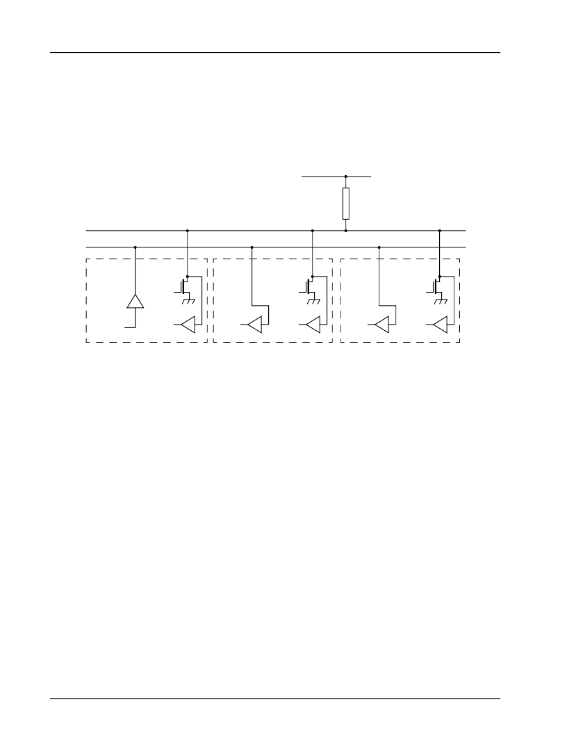
The CH7009 contains a standard I
2
C control port, through which the control registers can be written and read. This
port is comprised of a two-wire serial interface, pins SD (bidirectional) and SC, which can be connected directly to
the SDB and SCB buses as shown in
Figure 8
.
The Serial Clock line (SC) is input only and is driven by the output buffer of the master device (also shown in
Figure 8
). The CH7009 acts as a slave, and generation of clock signals on the bus is always the responsibility of the
master device. When the bus is free, both lines are HIGH. The output stages of devices connected to the bus must
have an open-drain or open-collector to perform the wired-AND function. Data on the bus can be transferred up to
400 kbit/s.
Figure 8: Connection of Devices to the Bus
Electrical Characteristics for Bus Devices
The electrical specifications of the bus devices’ inputs and outputs and the characteristics of the bus lines connected
to them are shown in
Figure 8
. A pull-up resistor (R
P
) must be connected to a 3.3V
±
10% supply. The CH7009 is
a device with input levels related to DVDD.
Maximum and minimum values of pull-up resistor (R
P
)
The value of R
P
depends on the following parameters:
Supply voltage
Bus capacitance
Number of devices connected (input current + leakage current = I
input
)
The supply voltage limits the minimum value of resistor R
P
due to the specified minimum sink current of 2mA at
VOL
max
= 0.4 V for the output stages:
R
P
>= (V
DD
– 0.4) / 2 (R
P
in k
)
The bus capacitance is the total capacitance of wire, connections and pins. This capacitance limits the maximum
value of R
P
due to the specified rise time. The equation for RP is shown below:
R
P
<= 10
3
/C (where: R
P
is in k
and C, the total capacitance, is in pF)
The maximum HIGH level input current of each input/output connection has a specified maximum value of 10
μ
A.
Due to the desired noise margin of 0.2V
DD
for the HIGH level, this input current limits the maximum value of R
P
.
The R
P
limit depends on V
DD
and is shown below:
R
P
<= (100 x V
DD
)/ I
input
(where: R
P
is in k
and I
input
is in
μ
A)
SCLK
IN2
DATA
IN2
DATAN2
OUT
SCB (Serial Clock Bus)
SDB (Serial Data Bus)
+DVDD
R
P
SLAVE
SCLK
IN1
DATA
IN1
DATAN2
OUT
SLAVE
SCLK
OUT
FROM
MASTER
DATA IN
MASTER
DATAN2
OUT
MASTER
BUS MASTER
SC
SD
相关PDF资料 |
PDF描述 |
|---|---|
| CH7303 | Chrontel CH7303 HDTV / DVI Encoder |
| CH8398A | TRUE-COLOR CHRONDAC WITH 16-BIT INTERFACE |
| CHF1206CNT | 20 W Power RF Chip Termination |
| CHF1206CNT500LY | 20 W Power RF Chip Termination |
| CHF1206CNT500LZ | 20 W Power RF Chip Termination |
相关代理商/技术参数 |
参数描述 |
|---|---|
| CH7011A-T | 制造商:未知厂家 制造商全称:未知厂家 功能描述:Consumer IC |
| CH7012 | 制造商:未知厂家 制造商全称:未知厂家 功能描述:Chrontel CH7012 TV Output Device |
| CH7012A | 制造商:未知厂家 制造商全称:未知厂家 功能描述:Chrontel CH7012 TV Output Device |
| CH7012A-T | 制造商:未知厂家 制造商全称:未知厂家 功能描述:Chrontel CH7012 TV Output Device |
| CH7013A | 制造商:未知厂家 制造商全称:未知厂家 功能描述:Digital PC to TV Encoder |
发布紧急采购,3分钟左右您将得到回复。