- 您现在的位置:买卖IC网 > PDF目录378829 > CH7009A (Electronic Theatre Controls, Inc.) Chrontel CH7009 DVI / TV Output Device PDF资料下载
参数资料
| 型号: | CH7009A |
| 厂商: | Electronic Theatre Controls, Inc. |
| 英文描述: | Chrontel CH7009 DVI / TV Output Device |
| 中文描述: | 昆泰CH7009和DVI / TV输出设备 |
| 文件页数: | 1/46页 |
| 文件大小: | 580K |
| 代理商: | CH7009A |
当前第1页第2页第3页第4页第5页第6页第7页第8页第9页第10页第11页第12页第13页第14页第15页第16页第17页第18页第19页第20页第21页第22页第23页第24页第25页第26页第27页第28页第29页第30页第31页第32页第33页第34页第35页第36页第37页第38页第39页第40页第41页第42页第43页第44页第45页第46页
CHRONTEL
201-0000-035 Rev 1.1, 5/8/2000 *TMDS is Trademark of Silicon Image Inc.
1
CH7009A
Chrontel CH7009 DVI / TV Output Device
Features
DVI Transmitter up to 165MHz
DVI low jitter PLL
DVI hot plug detection
TV output supporting up to 1024x768 graphics
resolutions
Macrovision
TM
7.X copy protection support
Programmable digital interface supports RGB and
YCrCb
TrueScale
TM
rendering engine supports underscan in all
TV output resolutions
Enhanced text sharpness and adaptive flicker removal
with up to 7 lines of filtering
Support for all NTSC and PAL formats
Provides CVBS, S-Video and SCART (RGB) outputs
TV connection detect
Programmable power management
10-bit video DAC outputs
Fully programmable through I
2
C port
Complete Windows and DOS driver support
Low voltage interface support to graphics device
Offered in a 64-pin LQFP package
General Description
The CH7009 is a Display controller device which accepts a
digital graphics input signal, and encodes and transmits
data through a DVI TMDS
TM
link (DFP can also be
supported) or TV output (analog composite, s-video or
RGB). The device accepts data over one 12-bit wide
variable voltage data port which supports five different
data formats including RGB and YCrCb.
The DVI processor includes a low jitter PLL for generation
of the high frequency serialize clock, and all circuitry
required to encode, serialize and transmit data. The
CH7009 comes in versions able to drive a DVI display at a
pixel rate of up to 165MHz, supporting UXGA resolution
displays. No scaling of input data is performed on the data
output to the DVI device.
The TV-Out processor will perform non-interlace to
interlace conversion with scaling and flicker filters, and
encode the data into any of the NTSC or PAL video
standards. The scaling and flicker filter is adaptive and
programmable to enable superior text display. Eight
graphics resolutions are supported up to 1024 by 768 with
full vertical and horizontal underscan capability in all
modes. A high accuracy low jitter phase locked loop is
integrated to create outstanding video quality. Support is
provided for Macrovision
TM
and RGB bypass mode which
enables driving a VGA CRT with the input data.
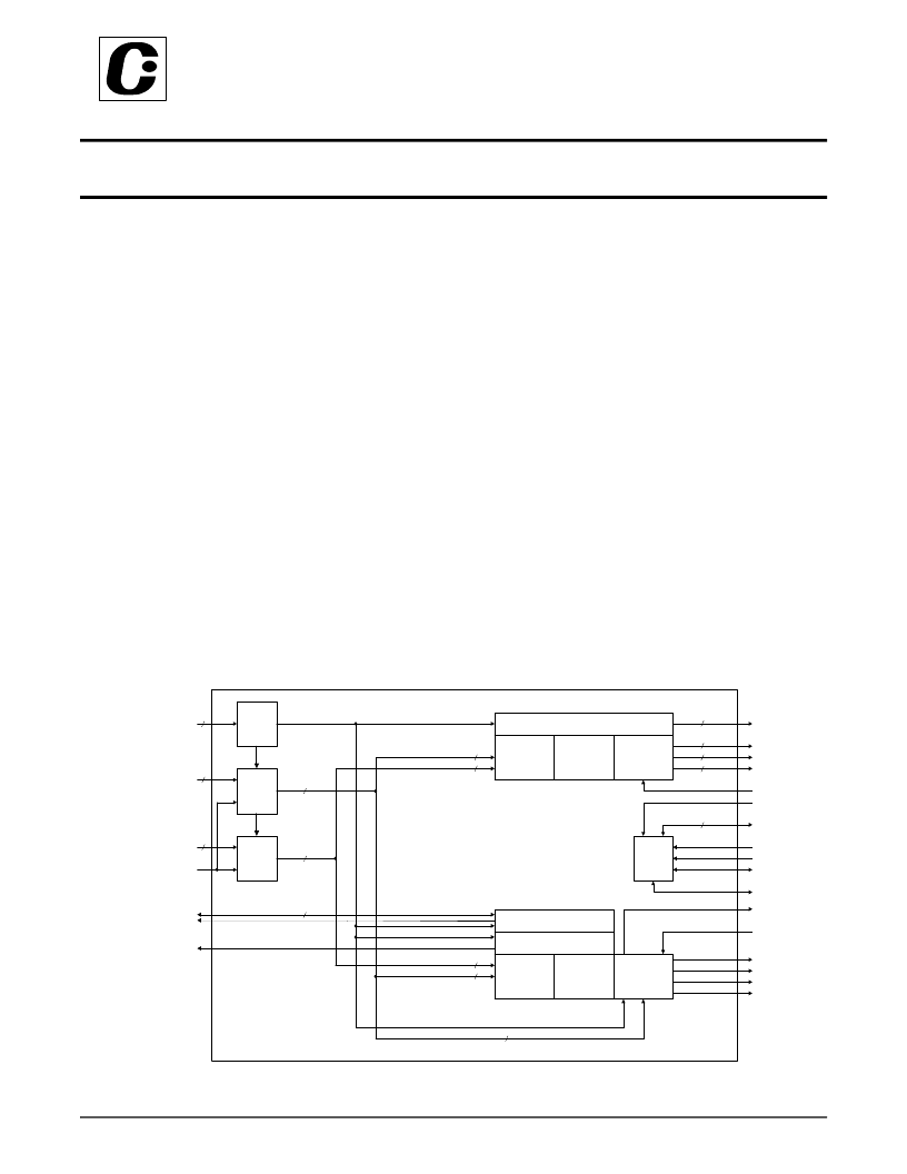
Figure 1: Functional Block Diagram
XCLK,XCLK*
IIC
Control
D[11:0]
H,V,DE
Data
Latch,
Demux
3
12
TDC2,TDC2*
TDC1,TDC1*
TDC0,TDC0*
TLC,TLC*
H,V,DE
Latch
DVI
Encode
DVI
Serialize
DVI
Driver
DVI (TMDS
TM
link) PLL
HPDET
3
24
Clock
Driver
AS
SC
SD
VREF
GPIO[1:0]
RESET*
XI/FIN,XO
CVBS
(DAC0)
C
(DAC 2)
Y
(DAC 1)
P-OUT / TLDET*
Four
10-bit
DAC's
3
24
BCO
C/H SYNC
ISET
Scaling
Scan Conv
Flicker Filt
TV
Encode
PLL3
Timing
CVBS
(DAC3)
VSWING
24
2
3
24
2
2
2
2
2
2
相关PDF资料 |
PDF描述 |
|---|---|
| CH7009A-T | Chrontel CH7009 DVI / TV Output Device |
| CH7303 | Chrontel CH7303 HDTV / DVI Encoder |
| CH8398A | TRUE-COLOR CHRONDAC WITH 16-BIT INTERFACE |
| CHF1206CNT | 20 W Power RF Chip Termination |
| CHF1206CNT500LY | 20 W Power RF Chip Termination |
相关代理商/技术参数 |
参数描述 |
|---|---|
| CH7009A-T | 制造商:未知厂家 制造商全称:未知厂家 功能描述:Chrontel CH7009 DVI / TV Output Device |
| CH7011A-T | 制造商:未知厂家 制造商全称:未知厂家 功能描述:Consumer IC |
| CH7012 | 制造商:未知厂家 制造商全称:未知厂家 功能描述:Chrontel CH7012 TV Output Device |
| CH7012A | 制造商:未知厂家 制造商全称:未知厂家 功能描述:Chrontel CH7012 TV Output Device |
| CH7012A-T | 制造商:未知厂家 制造商全称:未知厂家 功能描述:Chrontel CH7012 TV Output Device |
发布紧急采购,3分钟左右您将得到回复。