- 您现在的位置:买卖IC网 > Datasheet目录319 > CPD250-4530G (Power-One)PWR SUP 250W 3.3/5/12/-12V QUAD Datasheet资料下载
参数资料
| 型号: | CPD250-4530G |
| 厂商: | Power-One |
| 文件页数: | 11/19页 |
| 文件大小: | 0K |
| 描述: | PWR SUP 250W 3.3/5/12/-12V QUAD |
| 标准包装: | 20 |
| 系列: | CPD |
| 类型: | 隔离 |
| 输入电压: | 36 ~ 75V |
| 输出: | 5V,3.3V,±12V |
| 输出数: | 4 |
| 输出 - 1 @ 电流(最大): | 5 VDC @ 40A |
| 输出 - 2 @ 电流(最大): | 3.3 VDC @ 40A |
| 输出 - 3 @ 电流(最大): | 12 VDC @ 5.5A |
| 输出 - 4 @ 电流(最大): | -12 VDC @ 2A |
| 功率(瓦特): | 250W |
| 安装类型: | Compact PCI® |
| 效率: | 82.2% |
| 封装/外壳: | 模块 |
| 尺寸/尺寸: | 6.40" L x 1.60" W x 5.07" H(162.5mm x 40.6mm x 128.7mm) |
| 包装: | 散装 |
| 电源(瓦特)- 最大: | 250W |
| 批准: | CE,CSA,cUL,EN,TUV,UL |
| 产品目录页面: | 2739 (CN2011-ZH PDF) |
| 其它名称: | 179-2281 CPD250-4530-G |
�� �
�
�CPA,� CPD� Series� Data� Sheet�
�?�
�200� –� 550� Watt�
�CompactPCI� ?�
�AC-DC� and� DC-DC� Converters�
�Note� :� V� i� min� of� CPA� models� is� considered� as� insufficient,� when�
�V� i� remains� for� typ.� 30� ms� below� √� 2� ?� V� i� min� .�
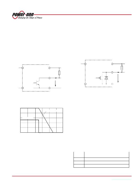
�Temperature Warning and Shutdown�
�A� temperature� warning� circuitry� monitors� the� case�
�temperature� T� C� .� Its� output� signal� V� DEG� #� changes� from� high� to�
�low� impedance,� when� the� T� C� exceeds� the� upper� threshold�
�level,� and� changes� back� to� high� impedance,� when� T� C� falls�
�below� the� lower� threshold� level,� which� is� 85� °C� ±� 5� °C.�
�Pin� 38� (degrade� signal� DEG#)� is� internally� connected� via� the�
�collector-emitter� path� of� an� NPN� transistor� to� the� signal� return�
�pin� 22.� The� current� I� DEG� #� through� pin� 38� should� not� exceed� 40�
�mA,� and� V� DEG#� should� not� exceed� 40� V.�
�If� T� C� exceeds� 105� °C,� the� converter� will� be� disabled.� It�
�The� threshold� levels� for� V� i� correspond� to� approx.� 34� V� for� CPD�
�models� and� 80� –� 90� VAC� for� CPA� models.�
�Note� :� CPD200/250� (and� CPA200/250� up� to� version� V116)�
�provide� only� the� signal� FAL#,� but� the� converter� is� not� inhibited.�
�–�
�Connector� pin� 42� (signal� V� FAL#� )� is� internally� connected� via� the�
�drain-source� path� of� a� JFET� (self-conducting� type)� to� the�
�signal� return� pin� 22.� The� current� I� FAL#� should� not� exceed�
�10� mA.� V� FAL#� should� not� exceed� 40� V,� as� the� JFET� is� not�
�protected� against� overvoltage.�
�resumes� operation� automatically,� once� T� C� falls� below� 105� °C.�
�JM110�
�46�
�11056a�
�38�
�Vo+�
�I� DEG#�
�DEG#�
�R� p�
�46�
�42�
�Vo+�
�I� FAL#�
�FAL#�
�V� FAL#�
�R� p�
�V� DEG#�
�47�
�22�
�47�
�22�
�RTN�
�RTN�
�Fig.� 8�
�Degrade� signal:� NPN� output� V� DEG� #� ≤� 40� V,� I� DEG� #� ≤� 20� mA�
�Fig.10�
�Power� Fail:� JFET� output,� I� FAL#� ≤� 10� mA�
�Sense� Lines�
�1�
�V� DEG#� [V]�
�10�
�8�
�P� o� /� P� o� max�
�05189c�
�thermal� shutdown�
�0.8�
�This� feature� is� available� only� for� the� outputs� Vo1,� Vo2,� Vo3,�
�and� allows� the� compensation� of� voltage� drops� across� the�
�connector� contacts� and� if� necessary,� across� the� load� lines.�
�To� ensure� correct� operation,� all� sense� lines� S+� (Vo1SENSE,�
�6�
�4�
�2�
�signal DEG#�
�0.6�
�0.4�
�0.2�
�Vo2SENSE,� and� Vo3SENSE)� should� be� connected� to� the�
�respective� power� outputs.� The� common� sense� return� S� –�
�(SRTN)� should� be� connected� to� RTN� (pin� 5� –� 12).�
�Note� :� Open� sense� lines� are� admissible,� but� the� output� voltage�
�regulation� will� be� poor.�
�The� voltage� difference� between� any� sense� line� at� its�
�0�
�60�
�70�
�80�
�90�
�100�
�110�
�°C�
�0�
�respective� power� output� pin� (as� measured� on� the� connector)�
�should� not� exceed� the� following� values.�
�Fig.� 9�
�Degrade� signal� V� DEG#� versus� case� temperature� T� C�
�Power� Fail� Signal�
�Note� :� If� the� sense� lines� S+� and� S–� compensate� for� a�
�considerable� voltage� drop,� the� output� loads� shall� be� reduced� in�
�order� to� respect� the� maximum� output� power.�
�Table� 7:� Sense� line� data�
�The� power� fail� circuitry� monitors� the� input� voltage� V� i� and� all�
�output� voltages.� The� signal� V� FAL#� changes� from� high� to� low�
�impedance� (<0.5� V),� when� one� of� the� monitored� voltages� falls�
�below� the� threshold.� V� FAL#� changes� back� to� high� impedance,�
�when� all� monitored� voltages� exceed� their� threshold� level.�
�The� threshold� level� for� V� o� corresponds� to� approx.� 90%� of�
�V� o� nom� .�
�Output�
�[V]�
�3.3�
�5�
�12�
�Total� voltage� difference� between� sense� lines�
�and� their� respective� outputs�
�0.8� V�
�1V�
�1V�
�BCD20005-G� Rev.� AG2,� 20-Dec-2012�
�Page� 11� of� 19�
�www.power-one.com�
�相关PDF资料 |
PDF描述 |
|---|---|
| CS4161YN8 | IC DRIVER H-BRDG DUAL 85MA 8DIP |
| CS5461A-ISZ | IC ENERGY METERING 1PHASE 24SSOP |
| CS5462-ISZ | IC ENERGY METERING 1PHASE 24SSOP |
| CS5463-IS | IC PWR/ENERGY METER 2CH 24-SSOP |
| CS5464-IS | IC PWR/ENERGY METER 3CH 28-SSOP |
相关代理商/技术参数 |
参数描述 |
|---|---|
| CPD250-4530-G | 制造商:Power-One 功能描述: |
| CPD250-4530GREP | 制造商:Power-One 功能描述: |
| CPD250-4530S188 | 制造商:Power-One 功能描述:- Bulk |
| CPD250-4530S201CG | 制造商:Power-One 功能描述: |
| CPD250-4530S201CGREP | 制造商:Power-One 功能描述: |
发布紧急采购,3分钟左右您将得到回复。