参数资料
| 型号: | CS2841BEDR14G |
| 厂商: | ON Semiconductor |
| 文件页数: | 6/10页 |
| 文件大小: | 0K |
| 描述: | IC REG CTRLR BST FLYBK CM 14SOIC |
| 产品变化通告: | Product Obsolescence 19/Jun/2009 |
| 标准包装: | 1 |
| PWM 型: | 电流模式 |
| 输出数: | 1 |
| 频率 - 最大: | 52kHz |
| 占空比: | 95% |
| 电源电压: | 7.8 V ~ 25 V |
| 降压: | 无 |
| 升压: | 是 |
| 回扫: | 是 |
| 反相: | 无 |
| 倍增器: | 无 |
| 除法器: | 无 |
| Cuk: | 无 |
| 隔离: | 无 |
| 工作温度: | -40°C ~ 85°C |
| 封装/外壳: | 14-SOIC(0.154",3.90mm 宽) |
| 包装: | 剪切带 (CT) |
| 其它名称: | CS2841BEDR14GOSCT |
�� �
�
�CS2841B�
�CIRCUIT� DESCRIPTION�
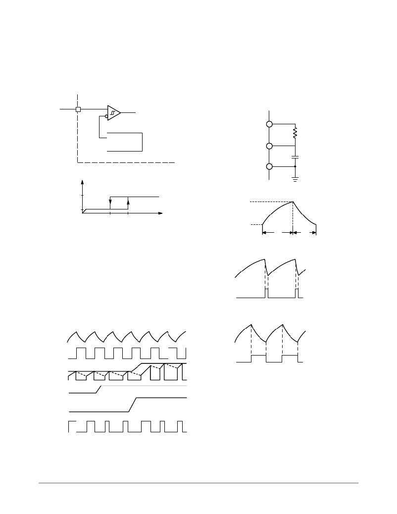
�Undervoltage� Lockout�
�During� Undervoltage� Lockout� (Figure� 5),� the� output�
�driver� is� biased� to� a� high� impedance� state.� The� output� should�
�be� shunted� to� ground� with� a� resistor� to� prevent� output�
�leakage� current� from� activating� the� power� switch.�
�When� the� power� supply� sees� a� sudden� large� output� current�
�increase,� the� control� voltage� will� increase� allowing� the� duty�
�cycle� to� momentarily� increase.� Since� the� duty� cycle� tends� to�
�exceed� the� maximum� allowed� to� prevent� transformer�
�saturation� in� some� power� supplies,� the� internal� oscillator�
�waveform� provides� the� maximum� duty� cycle� clamp� as�
�programmed� by� the� selection� of� OSC� components.�
�V� CC�
�ON/OFF� Command�
�to� Reset� of� IC�
�V� REF�
�V� ON� =� 8.0� V�
�V� OFF� =� 7.4� V�
�OSC�
�R� T�
�C� T�
�GND�
�I� CC�
�<� 15� mA�
�<� 1.0� mA�
�7.4� V�
�8.0� V�
�V� CC�
�Timing� Parameters�
�V� upper�
�V� lower�
�Figure� 5.� Typical� Undervoltage� Characteristics�
�Sawtooth� Mode�
�t� c�
�t� d�
�PWM� Waveform�
�To� generate� the� PWM� waveform,� the� control� voltage� from�
�the� error� amplifier� is� compared� to� a� current� sense� signal�
�representing� the� peak� output� inductor� current� (Figure� 6).� An�
�increase� in� V� CC� causes� the� inductor� current� slope� to�
�increase,� thus� reducing� the� duty� cycle.� This� is� an� inherent�
�feed-forward� characteristic� of� current� mode� control,� since�
�the� control� voltage� does� not� have� to� change� during� changes�
�of� input� supply� voltage.�
�Large� R� T� (� ≈� 10� k� W� )�
�Triangular� Mode�
�Small� R� T� (� ≈� 700� k� W� )�
�V� OSC�
�Internal� Clock�
�V� OSC�
�OSC�
�OSC�
�RESET�
�EA� Output�
�Switch�
�Current�
�Internal� Clock�
�Figure� 7.� Oscillator� Timing� Network� and�
�Parameters�
�V� CC�
�Setting� the� Oscillator�
�I� O�
�V� O�
�Figure� 6.� Timing� Diagram� for� Key� CS2841B�
�Parameters�
�Oscillator� timing� capacitor,� C� T� ,� is� charged� by� V� REF�
�through� R� T� and� discharged� by� an� internal� current� source.�
�During� the� discharge� time,� the� internal� clock� signal� blanks�
�out� the� output� to� the� Low� state,� thus� providing� a� user� selected�
�maximum� duty� cycle� clamp.� Charge� and� discharge� times� are�
�determined� by� the� general� formulas:�
�http://onsemi.com�
�6�
�相关PDF资料 |
PDF描述 |
|---|---|
| CS5101EN14G | IC REG BUCK 5V 1.5A 14DIP |
| CS51033GDR8G | IC REG CTRLR BUCK PWM 8-SOIC |
| CS51414GD8 | IC REG BUCK 1.5A 8SOIC |
| CS5157HGDR16G | IC CTRLR BUCK SYNC 5BIT 16-SOIC |
| CS5165AGDWR16G | IC CTRLR BUCK SYNC 5BIT 16-SOIC |
相关代理商/技术参数 |
参数描述 |
|---|---|
| CS2841BEN8 | 制造商:CHERRY 制造商全称:CHERRY 功能描述:Automotive Current Mode PWM Control Circuit |
| CS2842 | 制造商:未知厂家 制造商全称:未知厂家 功能描述: |
| CS28423AGD14 | 制造商:未知厂家 制造商全称:未知厂家 功能描述:Analog IC |
| CS28423AGD8 | 制造商:未知厂家 制造商全称:未知厂家 功能描述:Analog IC |
| CS28423AGDR14 | 制造商:未知厂家 制造商全称:未知厂家 功能描述:Analog IC |
发布紧急采购,3分钟左右您将得到回复。