- 您现在的位置:买卖IC网 > PDF目录9003 > CY28409AZXC (Silicon Laboratories Inc)IC CLOCK CK409GRANTSDALE 56TSSOP PDF资料下载
参数资料
| 型号: | CY28409AZXC |
| 厂商: | Silicon Laboratories Inc |
| 文件页数: | 16/16页 |
| 文件大小: | 0K |
| 描述: | IC CLOCK CK409GRANTSDALE 56TSSOP |
| 标准包装: | 35 |
| 类型: | * |
| PLL: | 是 |
| 输入: | 晶体 |
| 输出: | 时钟 |
| 电路数: | 1 |
| 比率 - 输入:输出: | 1:21 |
| 差分 - 输入:输出: | 无/是 |
| 频率 - 最大: | 400MHz |
| 除法器/乘法器: | 是/无 |
| 电源电压: | 3.135 V ~ 3.465 V |
| 工作温度: | 0°C ~ 70°C |
| 安装类型: | * |
| 封装/外壳: | * |
| 供应商设备封装: | * |
| 包装: | * |
CY28409
........................Document #: 38-07445 Rev. *D Page 9 of 16
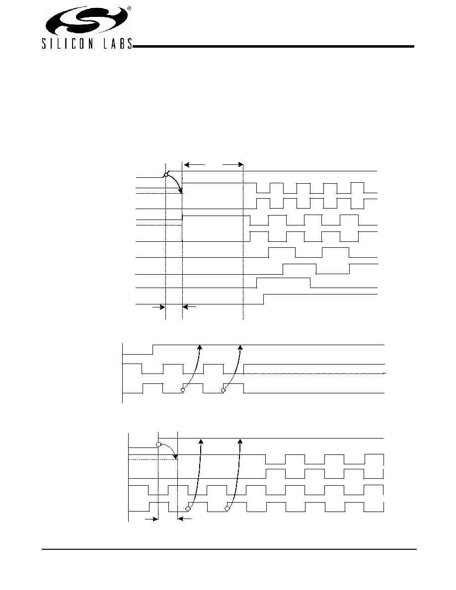
PD# Deassertion
The power-up latency between PD# rising to a valid logic ‘1’
level and the starting of all clocks is less than 1.8 ms.
CPU_STP# Assertion
The CPU_STP# signal is an active LOW input used for
synchronous stopping and starting the CPU output clocks
while the rest of the clock generator continues to function.
When the CPU_STP# pin is asserted, all CPU outputs that are
set with the SMBus configuration to be stoppable via assertion
of CPU_STP# will be stopped after being sampled by two
rising edges of the internal CPUT clock. The final states of the
stopped CPU signals are CPUT = HIGH and CPUC = LOW.
There is no change to the output drive current values during
the stopped state. The CPUT is driven HIGH with a current
value equal to (Mult 0 ‘select’) x (Iref), and the CPUC signal
will not be driven. Due to the external pull-down circuitry,
CPUC will be LOW during this stopped state.
CPU_STP# Deassertion
The deassertion of the CPU_STP# signal will cause all CPU
outputs that were stopped to resume normal operation in a
synchronous manner. Synchronous manner meaning that no
short or stretched clock pulses will be produce when the clock
resumes. The maximum latency from the deassertion to active
outputs is no more than two CPU clock cycles.
REF
Tdrive_PWRDN#
<300
s, >200 mV
PD#
CPUC, 133MHz
CPUT, 133MHz
SRCC 100MHz
3V66, 66MHz
USB, 48MHz
PCI, 33MHz
SRCT 100MHz
Tstable
<1.8 ms
Figure 4. Power-down Deassertion Timing Waveform
CPU_STP#
CPUT
CPUC
Figure 5. CPU_STP# Assertion Waveform
CPU_STP#
CPUT
CPUC
CPU Internal
Tdrive_CPU_STP#, 10 ns > 200 mV
Figure 6. CPU_STP# Deassertion Waveform
相关PDF资料 |
PDF描述 |
|---|---|
| VE-B4H-MY-F3 | CONVERTER MOD DC/DC 52V 50W |
| VE-B4H-MY-F2 | CONVERTER MOD DC/DC 52V 50W |
| VE-B4F-MY-F4 | CONVERTER MOD DC/DC 72V 50W |
| VE-B4F-MY-F3 | CONVERTER MOD DC/DC 72V 50W |
| MPC9773AER2 | IC PLL CLK GEN 1:12 3.3V 52-LQFP |
相关代理商/技术参数 |
参数描述 |
|---|---|
| CY28409AZXCT | 功能描述:时钟发生器及支持产品 SysClk Intel Grntsdl 865 and 875 chipsets RoHS:否 制造商:Silicon Labs 类型:Clock Generators 最大输入频率:14.318 MHz 最大输出频率:166 MHz 输出端数量:16 占空比 - 最大:55 % 工作电源电压:3.3 V 工作电源电流:1 mA 最大工作温度:+ 85 C 安装风格:SMD/SMT 封装 / 箱体:QFN-56 |
| CY28409OC | 功能描述:时钟合成器/抖动清除器 SysClk Intel Grntsdl 865 and 875 chipsets RoHS:否 制造商:Skyworks Solutions, Inc. 输出端数量: 输出电平: 最大输出频率: 输入电平: 最大输入频率:6.1 GHz 电源电压-最大:3.3 V 电源电压-最小:2.7 V 封装 / 箱体:TSSOP-28 封装:Reel |
| CY28409OCT | 功能描述:时钟合成器/抖动清除器 SysClk Intel Grntsdl 865 and 875 chipsets RoHS:否 制造商:Skyworks Solutions, Inc. 输出端数量: 输出电平: 最大输出频率: 输入电平: 最大输入频率:6.1 GHz 电源电压-最大:3.3 V 电源电压-最小:2.7 V 封装 / 箱体:TSSOP-28 封装:Reel |
| CY28409OCXT | 制造商:CYPRESS 制造商全称:Cypress Semiconductor 功能描述:Clock Synthesizer with Differential SRC and CPU Outputs |
| CY28409OXC | 功能描述:时钟合成器/抖动清除器 SysClk Intel Grntsdl 865 and 875 chipsets RoHS:否 制造商:Skyworks Solutions, Inc. 输出端数量: 输出电平: 最大输出频率: 输入电平: 最大输入频率:6.1 GHz 电源电压-最大:3.3 V 电源电压-最小:2.7 V 封装 / 箱体:TSSOP-28 封装:Reel |
发布紧急采购,3分钟左右您将得到回复。