- 您现在的位置:买卖IC网 > PDF目录9003 > MPC9773AER2 (IDT, Integrated Device Technology Inc)IC PLL CLK GEN 1:12 3.3V 52-LQFP PDF资料下载
参数资料
| 型号: | MPC9773AER2 |
| 厂商: | IDT, Integrated Device Technology Inc |
| 文件页数: | 1/21页 |
| 文件大小: | 0K |
| 描述: | IC PLL CLK GEN 1:12 3.3V 52-LQFP |
| 标准包装: | 1,500 |
| 类型: | PLL 时钟发生器 |
| PLL: | 带旁路 |
| 输入: | LVCMOS,LVPECL |
| 输出: | LVCMOS |
| 电路数: | 1 |
| 比率 - 输入:输出: | 3:12 |
| 差分 - 输入:输出: | 是/无 |
| 频率 - 最大: | 242.5MHz |
| 除法器/乘法器: | 是/无 |
| 电源电压: | 3.135 V ~ 3.465 V |
| 工作温度: | -40°C ~ 85°C |
| 安装类型: | 表面贴装 |
| 封装/外壳: | 52-LQFP |
| 供应商设备封装: | 52-TQFP(10x10) |
| 包装: | 带卷 (TR) |
DATASHEET
3.3 V 1:12 LVCMOS PLL Clock Generator
MPC9773
NRND
MPC9773 REVISION 6 JANUARY 31, 2013
1
2013 Integrated Device Technology, Inc.
The MPC9773 is a 3.3 V compatible, 1:12 PLL based clock generator targeted
for high-performance low-skew clock distribution in mid-range to high-
performance networking, computing, and telecom applications. With output
frequencies up to 240 MHz and output skews less than 250 ps the device meets
the needs of the most demanding clock applications.
Features
1:12 PLL based low-voltage clock generator
3.3 V power supply
Internal power-on reset
Generates clock signals up to 242.5 MHz
Maximum output skew of 250 ps
Differential PECL reference clock input
Two LVCMOS PLL reference clock inputs
External PLL feedback supports zero-delay capability
Various feedback and output dividers (refer to Application Section)
Supports up to three individual generated output clock frequencies
Synchronous output clock stop circuitry for each individual output for power
down support
Drives up to 24 clock lines
Ambient temperature range -40
C to +85C
Pin and function compatible to the MPC973
52-lead Pb-free package
NRND – Not Recommend for New Designs
Use replacement part ICS87973I
Functional Description
The MPC9773 utilizes PLL technology to frequency lock its outputs onto an
input reference clock. Normal operation of the MPC9773 requires the connection of the PLL feedback output QFB to feedback
input FB_IN to close the PLL feedback path. The reference clock frequency and the divider for the feedback path determine the
VCO frequency. Both must be selected to match the VCO frequency range. The MPC9773 features an extensive level of frequen-
cy programmability between the 12 outputs as well as the output to input relationships, for instance 1:1, 2:1, 3:1, 3:2, 4:1, 4:3,
5:1, 5:2, 5:3, 5:4, 5:6, 6:1, 8:1 and 8:3.
The QSYNC output will indicate when the coincident rising edges of the above relationships will occur. The selectability of the
feedback frequency is independent of the output frequencies. This allows for very flexible programming of the input reference
versus output frequency relationship. The output frequencies can be either odd or even multiples of the input reference. In addi-
tion, the output frequency can be less than the input frequency for applications where a frequency needs to be reduced by a non-
binary factor. The MPC9773 also supports the 180
phase shift of one of its output banks with respect to the other output banks.
The QSYNC outputs reflect the phase relationship between the QA and QC outputs and can be used for the generation of system
baseline timing signals.
The REF_SEL pin selects the LVPECL or the LVCMOS compatible inputs as the reference clock signal. Two alternative
LVCMOS compatible clock inputs are provided for clock redundancy support. The PLL_EN control selects the PLL bypass con-
figuration for test and diagnosis. In this configuration, the selected input reference clock is routed directly to the output dividers,
bypassing the PLL. The PLL bypass is fully static and the minimum clock frequency specification and all other PLL characteristics
do not apply.
The outputs can be individually disabled (stopped in logic low state) by programming the serial CLOCK_STOP interface of the
MPC9773. The MPC9773 has an internal power-on reset.
The MPC9773 is fully 3.3 V compatible and requires no external loop filter components. All inputs (except PCLK) accept
LVCMOS signals while the outputs provide LVCMOS compatible levels with the capability to drive terminated 50
transmission
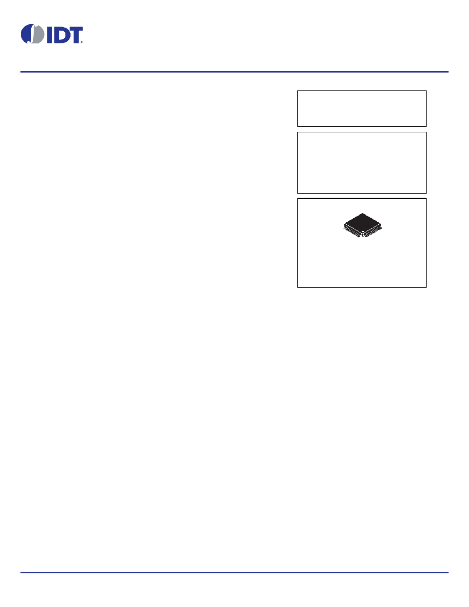
AE SUFFIX
52-LEAD LQFP PACKAGE
Pb-FREE PACKAGE
CASE 848D-03
MPC9773
3.3 V 1:12 LVCMOS
PLL CLOCK GENERATOR
NRND – Not Recommend for New Designs
相关PDF资料 |
PDF描述 |
|---|---|
| VE-B4D-MY-F2 | CONVERTER MOD DC/DC 85V 50W |
| VE-B4D-MY-F1 | CONVERTER MOD DC/DC 85V 50W |
| MS27473T24F2S | CONN PLUG 100POS STRAIGHT W/SCKT |
| VE-BNL-MV-F1 | CONVERTER MOD DC/DC 28V 150W |
| VE-BNK-MV-F4 | CONVERTER MOD DC/DC 40V 150W |
相关代理商/技术参数 |
参数描述 |
|---|---|
| MPC9773FA | 功能描述:锁相环 - PLL 3.3V 240MHz Clock Generator RoHS:否 制造商:Silicon Labs 类型:PLL Clock Multiplier 电路数量:1 最大输入频率:710 MHz 最小输入频率:0.002 MHz 输出频率范围:0.002 MHz to 808 MHz 电源电压-最大:3.63 V 电源电压-最小:1.71 V 最大工作温度:+ 85 C 最小工作温度:- 40 C 封装 / 箱体:QFN-36 封装:Tray |
| MPC9773FAR2 | 制造商:Integrated Device Technology Inc 功能描述:PLL Clock Driver Single 52-Pin LQFP T/R 制造商:Integrated Device Technology Inc 功能描述:MPC9773FAR2 - Tape and Reel |
| MPC9774 | 制造商:MOTOROLA 制造商全称:Motorola, Inc 功能描述:3.3V / 2,5V 1:14 LVCMOS PLL CLOCK GENERATOR |
| MPC9774AE | 功能描述:时钟发生器及支持产品 3.3V 125MHz Clock Generator RoHS:否 制造商:Silicon Labs 类型:Clock Generators 最大输入频率:14.318 MHz 最大输出频率:166 MHz 输出端数量:16 占空比 - 最大:55 % 工作电源电压:3.3 V 工作电源电流:1 mA 最大工作温度:+ 85 C 安装风格:SMD/SMT 封装 / 箱体:QFN-56 |
| MPC9774AER2 | 功能描述:IC PLL CLK GEN 1:14 3.3V 52-LQFP RoHS:是 类别:集成电路 (IC) >> 时钟/计时 - 时钟发生器,PLL,频率合成器 系列:- 标准包装:1,000 系列:- 类型:时钟/频率合成器,扇出分配 PLL:- 输入:- 输出:- 电路数:- 比率 - 输入:输出:- 差分 - 输入:输出:- 频率 - 最大:- 除法器/乘法器:- 电源电压:- 工作温度:- 安装类型:表面贴装 封装/外壳:56-VFQFN 裸露焊盘 供应商设备封装:56-VFQFP-EP(8x8) 包装:带卷 (TR) 其它名称:844S012AKI-01LFT |
发布紧急采购,3分钟左右您将得到回复。