- 您现在的位置:买卖IC网 > PDF目录9003 > MPC9773AER2 (IDT, Integrated Device Technology Inc)IC PLL CLK GEN 1:12 3.3V 52-LQFP PDF资料下载
参数资料
| 型号: | MPC9773AER2 |
| 厂商: | IDT, Integrated Device Technology Inc |
| 文件页数: | 20/21页 |
| 文件大小: | 0K |
| 描述: | IC PLL CLK GEN 1:12 3.3V 52-LQFP |
| 标准包装: | 1,500 |
| 类型: | PLL 时钟发生器 |
| PLL: | 带旁路 |
| 输入: | LVCMOS,LVPECL |
| 输出: | LVCMOS |
| 电路数: | 1 |
| 比率 - 输入:输出: | 3:12 |
| 差分 - 输入:输出: | 是/无 |
| 频率 - 最大: | 242.5MHz |
| 除法器/乘法器: | 是/无 |
| 电源电压: | 3.135 V ~ 3.465 V |
| 工作温度: | -40°C ~ 85°C |
| 安装类型: | 表面贴装 |
| 封装/外壳: | 52-LQFP |
| 供应商设备封装: | 52-TQFP(10x10) |
| 包装: | 带卷 (TR) |
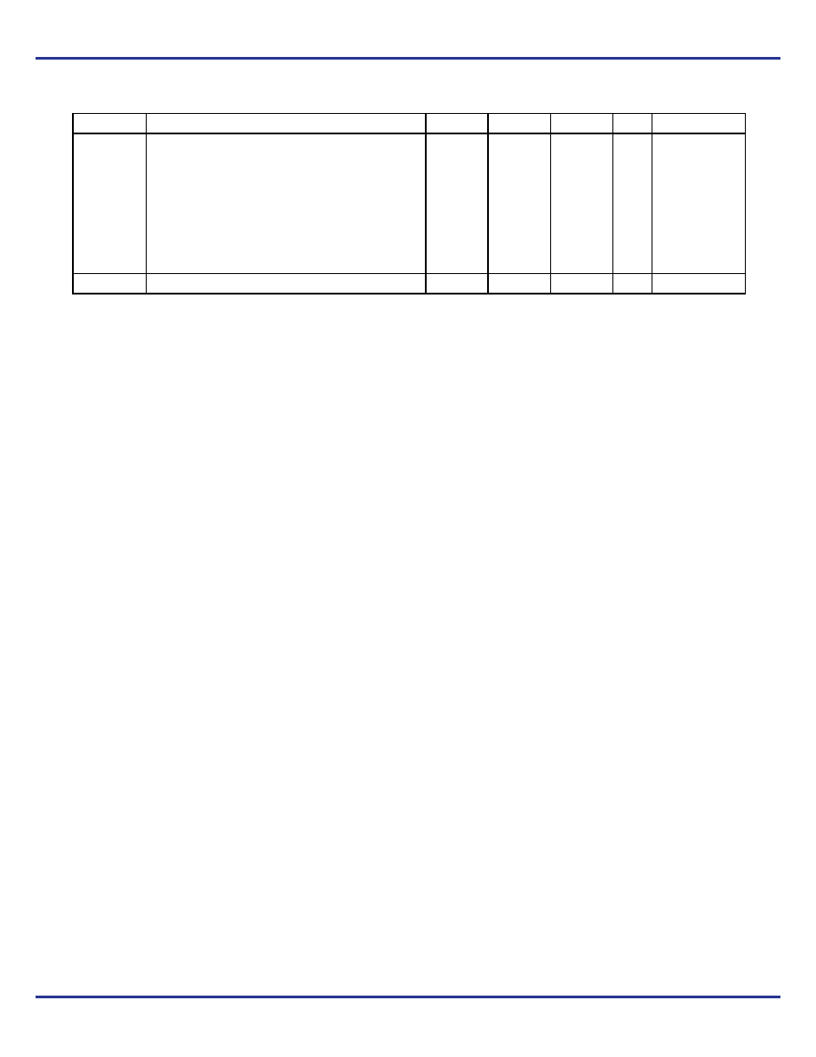
MPC9773 REVISION 6 JANUARY 31, 2013
8
2013 Integrated Device Technology, Inc.
MPC9773 Data Sheet
3.3 V 1:12 LVCMOS PLL CLOCK GENERATOR
BW
PLL Closed Loop Bandwidth(12)
4 feedback
6 feedback
8 feedback
10 feedback
12 feedback
16 feedback
20 feedback
24 feedback
32 feedback
40 feedback
1.20 – 3.50
0.70 – 2.50
0.50 – 1.80
0.45 – 1.20
0.30 – 1.00
0.25 – 0.70
0.20 – 0.55
0.17 – 0.40
0.12 – 0.30
0.11 – 0.28
MHz
tLOCK
Maximum PLL Lock Time
10
ms
1. AC characteristics apply for parallel output termination of 50
to VTT.
2. The input reference frequency must match the VCO lock range divided by the feedback divider ratio: fREF = fVCO (M VCO_SEL).
3. VCMR (AC) is the crosspoint of the differential input signal. Normal AC operation is obtained when the crosspoint is within the VCMR range
and the input swing lies within the VPP (AC) specification. Violation of VCMR or VPP impacts static phase offset t().
4. Calculation of reference duty cycle limits: DCREF,MIN = tPW,MIN fREF 100% and DCREF,MAX = 100% – DCREF,MIN.
5. The MPC9773 will operate with input rise/fall times up to 3.0 ns, but the AC characteristics, specifically t(), tPW,MIN, DC and fMAX can only
be guaranteed if tR, tF are within the specified range.
6. CCLKx or PCLK to FB_IN. Static phase offset depends on the reference frequency. t() [s] = t() [] (fREF 360).
7. Excluding QSYNC output. Refer to APPLICATIONS INFORMATION for part-to-part skew calculation.
8. Output duty cycle is DC = (0.5
200 ps fOUT) 100%. E.g., the DC range at fOUT = 100 MHz is 48% < DC < 52%. T = output period.
9. Cycle jitter is valid for all outputs in the same divider configuration.
10. Period jitter is valid for all outputs in the same divider configuration.
11. I/O jitter is valid for a VCO frequency of 400 MHz. Refer to APPLICATIONS INFORMATION for I/O jitter vs. VCO frequency.
12. –3 dB point of PLL transfer characteristics.
Table 10. AC Characteristics (VCC = 3.3 V ± 5%, TA = -40°C to 85°C)(1), (2)
Symbol
Characteristics
Min
Typ
Max
Unit
Condition
相关PDF资料 |
PDF描述 |
|---|---|
| VE-B4D-MY-F2 | CONVERTER MOD DC/DC 85V 50W |
| VE-B4D-MY-F1 | CONVERTER MOD DC/DC 85V 50W |
| MS27473T24F2S | CONN PLUG 100POS STRAIGHT W/SCKT |
| VE-BNL-MV-F1 | CONVERTER MOD DC/DC 28V 150W |
| VE-BNK-MV-F4 | CONVERTER MOD DC/DC 40V 150W |
相关代理商/技术参数 |
参数描述 |
|---|---|
| MPC9773FA | 功能描述:锁相环 - PLL 3.3V 240MHz Clock Generator RoHS:否 制造商:Silicon Labs 类型:PLL Clock Multiplier 电路数量:1 最大输入频率:710 MHz 最小输入频率:0.002 MHz 输出频率范围:0.002 MHz to 808 MHz 电源电压-最大:3.63 V 电源电压-最小:1.71 V 最大工作温度:+ 85 C 最小工作温度:- 40 C 封装 / 箱体:QFN-36 封装:Tray |
| MPC9773FAR2 | 制造商:Integrated Device Technology Inc 功能描述:PLL Clock Driver Single 52-Pin LQFP T/R 制造商:Integrated Device Technology Inc 功能描述:MPC9773FAR2 - Tape and Reel |
| MPC9774 | 制造商:MOTOROLA 制造商全称:Motorola, Inc 功能描述:3.3V / 2,5V 1:14 LVCMOS PLL CLOCK GENERATOR |
| MPC9774AE | 功能描述:时钟发生器及支持产品 3.3V 125MHz Clock Generator RoHS:否 制造商:Silicon Labs 类型:Clock Generators 最大输入频率:14.318 MHz 最大输出频率:166 MHz 输出端数量:16 占空比 - 最大:55 % 工作电源电压:3.3 V 工作电源电流:1 mA 最大工作温度:+ 85 C 安装风格:SMD/SMT 封装 / 箱体:QFN-56 |
| MPC9774AER2 | 功能描述:IC PLL CLK GEN 1:14 3.3V 52-LQFP RoHS:是 类别:集成电路 (IC) >> 时钟/计时 - 时钟发生器,PLL,频率合成器 系列:- 标准包装:1,000 系列:- 类型:时钟/频率合成器,扇出分配 PLL:- 输入:- 输出:- 电路数:- 比率 - 输入:输出:- 差分 - 输入:输出:- 频率 - 最大:- 除法器/乘法器:- 电源电压:- 工作温度:- 安装类型:表面贴装 封装/外壳:56-VFQFN 裸露焊盘 供应商设备封装:56-VFQFP-EP(8x8) 包装:带卷 (TR) 其它名称:844S012AKI-01LFT |
发布紧急采购,3分钟左右您将得到回复。