- 您现在的位置:买卖IC网 > PDF目录9582 > CY28445LFXC-5T (Silicon Laboratories Inc)IC CLOCK CALISTOGA CK410M 68QFN PDF资料下载
参数资料
| 型号: | CY28445LFXC-5T |
| 厂商: | Silicon Laboratories Inc |
| 文件页数: | 7/25页 |
| 文件大小: | 0K |
| 描述: | IC CLOCK CALISTOGA CK410M 68QFN |
| 标准包装: | 2,000 |
| 类型: | 时钟/频率发生器 |
| PLL: | 是 |
| 主要目的: | Intel CPU 服务器 |
| 输入: | LVTTL,晶体 |
| 输出: | HCSL,LVCMOS |
| 电路数: | 1 |
| 比率 - 输入:输出: | 3:22 |
| 差分 - 输入:输出: | 无/是 |
| 频率 - 最大: | 200MHz |
| 电源电压: | 3.135 V ~ 3.465 V |
| 工作温度: | 0°C ~ 85°C |
| 安装类型: | 表面贴装 |
| 封装/外壳: | 68-VFQFN 裸露焊盘 |
| 供应商设备封装: | 68-QFN(8x8) |
| 包装: | 带卷 (TR) |
CY28445-5
..................... Document #: 38-07739 Rev *C Page 15 of 25
CLKREQ# Assertion (CLKREQ# -> LOW)
All differential outputs that were stopped are to resume normal
operation in a glitch free manner. The maximum latency from
the assertion to active outputs is between 2–6 SRC clock
periods (2 clocks are shown) with all SRC outputs resuming
simultaneously. All stopped SRC outputs must be driven high
within 10 ns of CLKREQ# deassertion to a voltage greater than
200 mV.
CLKREQ# Deassertion (CLKREQ# -> HIGH)
The impact of deasserting the CLKREQ# pins is all SRC
outputs that are set in the control registers to stoppable via
deassertion of CLKREQ# are to be stopped after their next
transition. The final state of all stopped DIF signals is low, both
SRCT clock and SRCC clock outputs will not be driven.PD
(Power-down) Clarification
The VTT_PWRGD# /PD pin is a dual-function pin. During
initial power-up, the pin functions as VTT_PWRGD#. Once
VTT_PWRGD# has been sampled low by the clock chip, the
pin assumes PD functionality. The PD pin is an asynchronous
active high input used to shut off all clocks cleanly prior to
shutting off power to the device. This signal is synchronized
internal to the device prior to powering down the clock synthe-
sizer. PD is also an asynchronous input for powering up the
system. When PD is asserted high, all clocks need to be driven
to a low value and held prior to turning off the VCOs and the
crystal oscillator.
PD Assertion
When PD is sampled high by two consecutive rising edges of
CPUC, all single-ended outputs will be held low on their next
high to low transition and differential clocks must held high or
tri-stated (depending on the state of the control register drive
mode bit) on the next diff clock# high to low transition within 4
clock periods. When the SMBus PD drive mode bit corre-
sponding to the differential (CPU, SRC, and DOT) clock output
of interest is programmed to ‘0’, the clock output are held with
“Diff clock” pin driven high at 2 x Iref, and “Diff clock#” tristate.
If the control register PD drive mode bit corresponding to the
output of interest is programmed to “1”, then both the “Diff
clock” and the “Diff clock#” are tri-state. Note the example
below shows CPUT = 133 MHz and PD drive mode = ‘1’ for all
differential outputs. This diagram and description is applicable
to valid CPU frequencies 100, 133, 166, and 200 MHz. In the
event that PD mode is desired as the initial power-on state, PD
must be asserted high in less than 10
s after asserting
Vtt_PwrGd#. It should be noted that 96_100_SSC will follow
the DOT waveform is selected for 96 MHz and the SRC
waveform when in 100-MHz mode.
PD Deassertion
The power-up latency is less than 1.8 ms. This is the time from
the deassertion of the PD pin or the ramping of the power
supply until the time that stable clocks are output from the
clock chip. All differential outputs stopped in a three-state
condition resulting from power down will be driven high in less
than 300
s of PD deassertion to a voltage greater than
200 mV. After the clock chip’s internal PLL is powered up and
locked, all outputs will be enabled within a few clock cycles of
each other. Below is an example showing the relationship of
clocks coming up. It should be noted that 96_100_SSC will
follow the DOT waveform is selected for 96 MHz and the SRC
waveform when in 100-MHz mode.
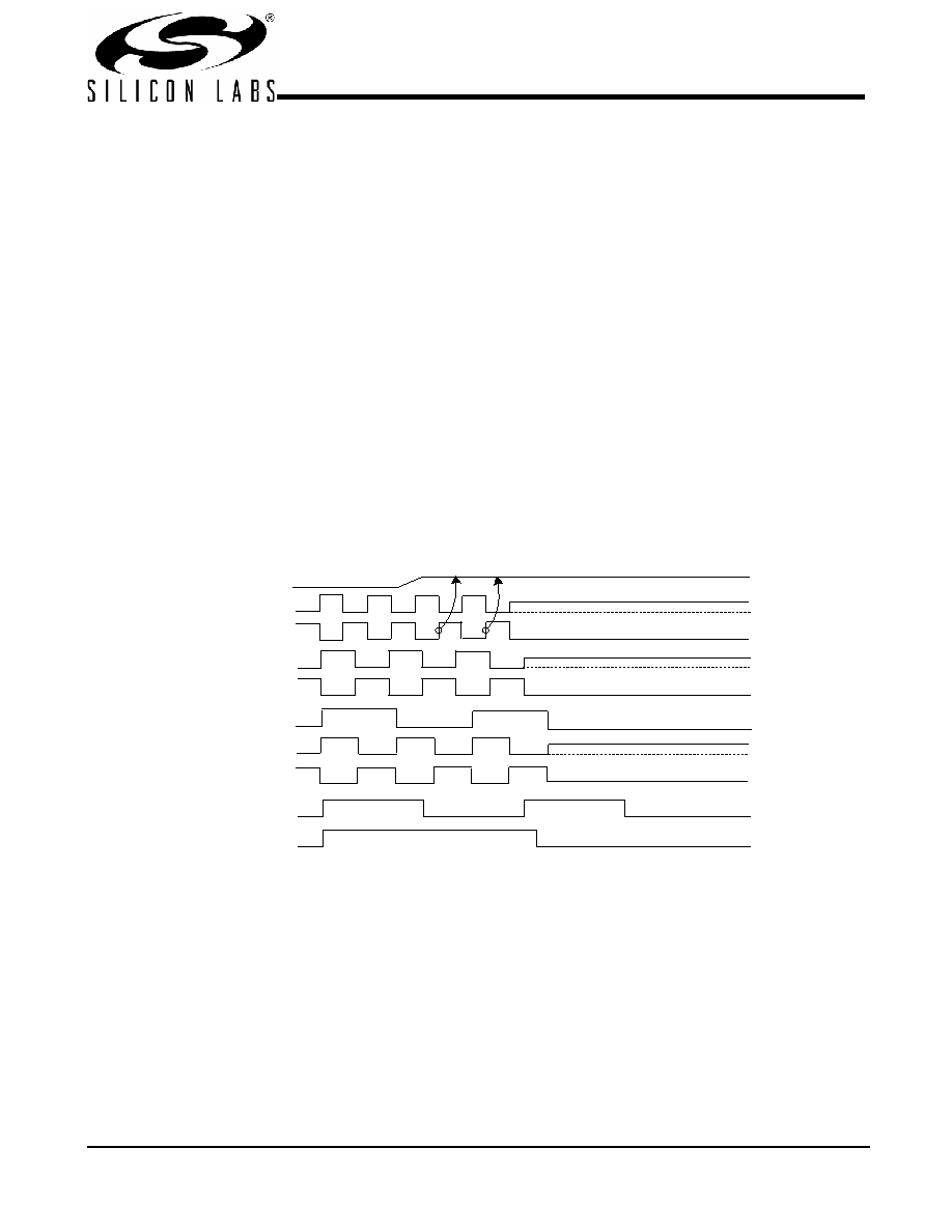
Figure 4. PD Assertion Timing Waveform
PD
U SB, 48M H z
DO T 96T
DO T 96C
S RCT 100M Hz
S RCC 100M Hz
CP UT , 133M Hz
P C I, 33 M H z
RE F
CP UC, 133M Hz
相关PDF资料 |
PDF描述 |
|---|---|
| VI-B4J-IU | CONVERTER MOD DC/DC 36V 200W |
| MC1489DR2G | IC LINE RECEIVER QUAD 14-SOIC |
| VI-B4F-IU | CONVERTER MOD DC/DC 72V 200W |
| VI-B31-MY-S | CONVERTER MOD DC/DC 12V 50W |
| MC1489DR2 | IC LINE RECEIVER QUAD 14-SOIC |
相关代理商/技术参数 |
参数描述 |
|---|---|
| CY28446 | 制造商:CYPRESS 制造商全称:Cypress Semiconductor 功能描述:Clock Generator for Intel㈢ Calistoga Chipset |
| CY28446LFXC | 功能描述:时钟发生器及支持产品 Calistoga RoHS:否 制造商:Silicon Labs 类型:Clock Generators 最大输入频率:14.318 MHz 最大输出频率:166 MHz 输出端数量:16 占空比 - 最大:55 % 工作电源电压:3.3 V 工作电源电流:1 mA 最大工作温度:+ 85 C 安装风格:SMD/SMT 封装 / 箱体:QFN-56 |
| CY28446LFXCT | 功能描述:时钟发生器及支持产品 Calistoga RoHS:否 制造商:Silicon Labs 类型:Clock Generators 最大输入频率:14.318 MHz 最大输出频率:166 MHz 输出端数量:16 占空比 - 最大:55 % 工作电源电压:3.3 V 工作电源电流:1 mA 最大工作温度:+ 85 C 安装风格:SMD/SMT 封装 / 箱体:QFN-56 |
| CY28447 | 制造商:SPECTRALINEAR 制造商全称:SPECTRALINEAR 功能描述:Clock Generator for Intel㈢ Calistoga Chipset |
| CY28447LFXC | 功能描述:时钟发生器及支持产品 Calistoga System Clk Extra SRC Output RoHS:否 制造商:Silicon Labs 类型:Clock Generators 最大输入频率:14.318 MHz 最大输出频率:166 MHz 输出端数量:16 占空比 - 最大:55 % 工作电源电压:3.3 V 工作电源电流:1 mA 最大工作温度:+ 85 C 安装风格:SMD/SMT 封装 / 箱体:QFN-56 |
发布紧急采购,3分钟左右您将得到回复。