- 您现在的位置:买卖IC网 > PDF目录8706 > CY2SSTV850ZC (Silicon Laboratories Inc)IC PLL BUF/DRIV I2C 1:10 48TSSOP PDF资料下载
参数资料
| 型号: | CY2SSTV850ZC |
| 厂商: | Silicon Laboratories Inc |
| 文件页数: | 2/9页 |
| 文件大小: | 0K |
| 描述: | IC PLL BUF/DRIV I2C 1:10 48TSSOP |
| 标准包装: | 39 |
| 类型: | * |
| PLL: | 带旁路 |
| 输入: | 时钟 |
| 输出: | 时钟 |
| 电路数: | 1 |
| 比率 - 输入:输出: | 1:10 |
| 差分 - 输入:输出: | 是/是 |
| 频率 - 最大: | 170MHz |
| 除法器/乘法器: | 无/无 |
| 电源电压: | 2.375 V ~ 3.465 V |
| 工作温度: | 0°C ~ 70°C |
| 安装类型: | * |
| 封装/外壳: | * |
| 供应商设备封装: | * |
| 包装: | * |
CY2SSTV850
......................... Document #: 38-07457 Rev. *A Page 2 of 9
Notes:
1. PU= internal pull-up
2. A bypass capacitor (0.1
F) should be placed as close as possible to each positive power pin (<0.2”). If these bypass capacitors are not close to the pins their
high-frequency filtering characteristic will be cancelled by the lead inductance of the traces
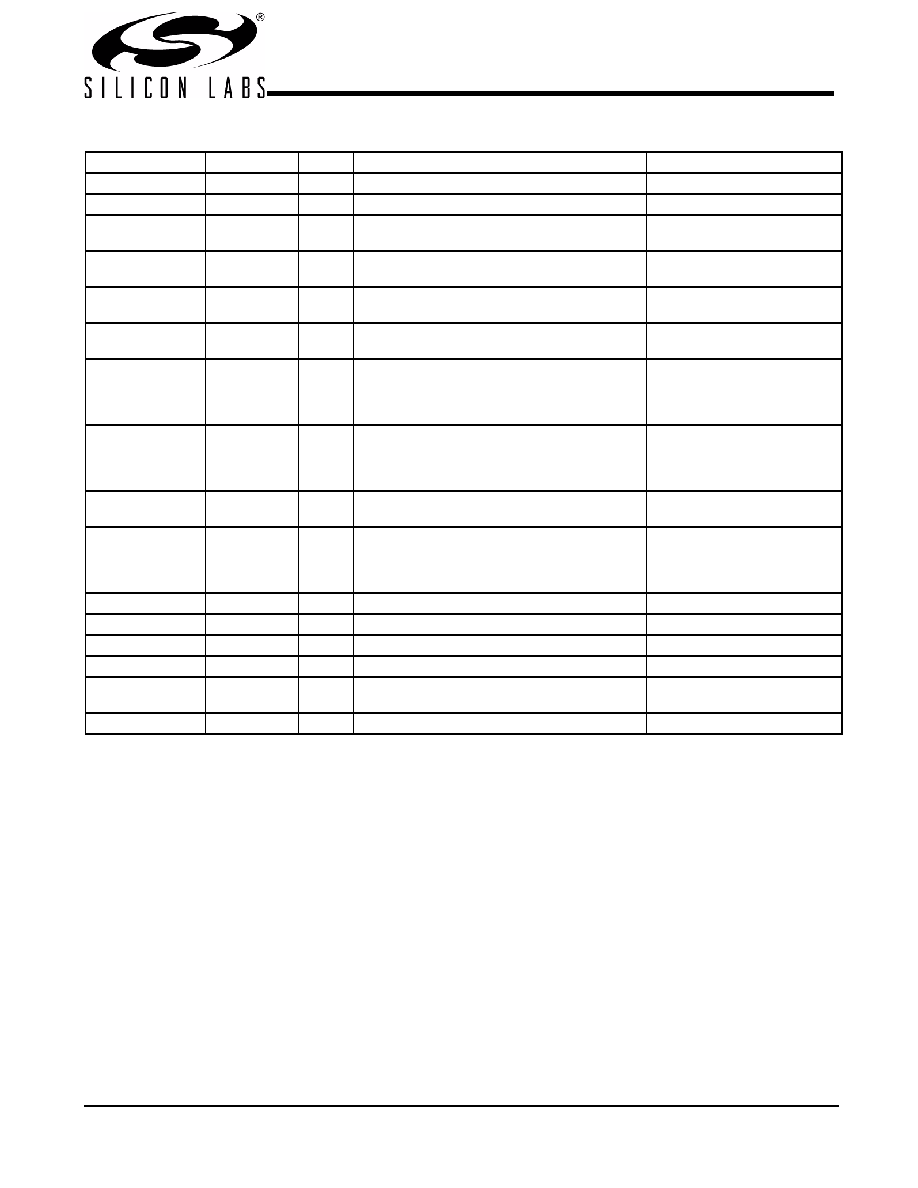
Pin Description[1, 2]
Pin
Name
I/O
Description
Electrical Characteristics
13
CLKINT
I
Complementary Clock Input.
LV Differential Input
14
CLKINC
I
Complementary Clock Input.
35
FBINC
I
Feedback Clock Input. Connect to FBOUTC for
accessing the PLL.
Differential Input
36
FBINT
I
Feedback Clock Input. Connect to FBOUTT for
accessing the PLL.
3, 5, 10, 20, 22
46, 44, 39, 29,27
YT(0:9)
O
Clock Outputs
Differential Outputs
2, 6, 9, 19, 23
47, 43, 40,30,26
YC(0:9)
O
Clock Outputs
32
FBOUTT
O
Feedback Clock Output. Connect to FBINT for
normal operation. A bypass delay capacitor at
this output will control Input Reference/Output
Clocks phase relationships.
Differential Outputs
33
FBOUTC
O
Feedback Clock Output. Connect to FBINC for
normal operation. A bypass delay capacitor at
this output will control Input Reference/Output
Clocks phase relationships.
12
SCLK
I, PU
Serial Clock Input. Clocks data at SDATA into
the internal register.
Data Input for the two-line serial
bus
37
SDATA
I/O, PU Serial Data Input. Input data is clocked to the
internal register to enable/disable individual
outputs. This provides flexibility in power
management.
Data Input and Output for the
two-line serial bus
11
VDD
2.5V power Supply for Logic
2.5V Nominal
4, 21, 28, 34, 38, 45 VDDQ
2.5V Power Supply for Output Clock Buffers 2.5V Nominal
16
AVDD
2.5V Power Supply for PLL
2.5V Nominal
15
VDDI
Power Supply for two-line serial Interface
2.5V or 3.3V Nominal
1, 7, 8, 18, 24, 25,
31, 41, 42, 48
VSS
Common Ground
0.0V Ground
17
AVSS
Analog Ground
0.0V Analog Ground
相关PDF资料 |
PDF描述 |
|---|---|
| V150A5H400B3 | CONVERTER MOD DC/DC 5V 400W |
| V110A36H400BF3 | CONVERTER MOD DC/DC 36V 400W |
| VE-JN3-MY | CONVERTER MOD DC/DC 24V 50W |
| VE-JN2-MY | CONVERTER MOD DC/DC 15V 50W |
| VE-JN1-MY | CONVERTER MOD DC/DC 12V 50W |
相关代理商/技术参数 |
参数描述 |
|---|---|
| CY2SSTV850ZCT | 功能描述:时钟缓冲器 2.5V 170MHz 1:10 Diff DDR PLL+I2C RoHS:否 制造商:Texas Instruments 输出端数量:5 最大输入频率:40 MHz 传播延迟(最大值): 电源电压-最大:3.45 V 电源电压-最小:2.375 V 最大功率耗散: 最大工作温度:+ 85 C 最小工作温度:- 40 C 封装 / 箱体:LLP-24 封装:Reel |
| CY2SSTV850ZI | 功能描述:时钟缓冲器 DDR1 Clock PLL RoHS:否 制造商:Texas Instruments 输出端数量:5 最大输入频率:40 MHz 传播延迟(最大值): 电源电压-最大:3.45 V 电源电压-最小:2.375 V 最大功率耗散: 最大工作温度:+ 85 C 最小工作温度:- 40 C 封装 / 箱体:LLP-24 封装:Reel |
| CY2SSTV850ZIT | 功能描述:时钟缓冲器 DDR1 Clock PLL RoHS:否 制造商:Texas Instruments 输出端数量:5 最大输入频率:40 MHz 传播延迟(最大值): 电源电压-最大:3.45 V 电源电压-最小:2.375 V 最大功率耗散: 最大工作温度:+ 85 C 最小工作温度:- 40 C 封装 / 箱体:LLP-24 封装:Reel |
| CY2SSTV855 | 制造商:CYPRESS 制造商全称:Cypress Semiconductor 功能描述:Differential Clock Buffer/Driver |
| CY2SSTV855_06 | 制造商:CYPRESS 制造商全称:Cypress Semiconductor 功能描述:Differential Clock Buffer/Driver |
发布紧急采购,3分钟左右您将得到回复。