- 您现在的位置:买卖IC网 > PDF目录8706 > CY2SSTV850ZC (Silicon Laboratories Inc)IC PLL BUF/DRIV I2C 1:10 48TSSOP PDF资料下载
参数资料
| 型号: | CY2SSTV850ZC |
| 厂商: | Silicon Laboratories Inc |
| 文件页数: | 6/9页 |
| 文件大小: | 0K |
| 描述: | IC PLL BUF/DRIV I2C 1:10 48TSSOP |
| 标准包装: | 39 |
| 类型: | * |
| PLL: | 带旁路 |
| 输入: | 时钟 |
| 输出: | 时钟 |
| 电路数: | 1 |
| 比率 - 输入:输出: | 1:10 |
| 差分 - 输入:输出: | 是/是 |
| 频率 - 最大: | 170MHz |
| 除法器/乘法器: | 无/无 |
| 电源电压: | 2.375 V ~ 3.465 V |
| 工作温度: | 0°C ~ 70°C |
| 安装类型: | * |
| 封装/外壳: | * |
| 供应商设备封装: | * |
| 包装: | * |
CY2SSTV850
......................... Document #: 38-07457 Rev. *A Page 6 of 9
Note:
11. Parameters are guaranteed by design and characterization. Not 100% tested in production.
12. PLL is capable of meeting the specified parameters while supporting SSC synthesizers with modulation frequency between 30 kHz and 33.3 kHz with a down
spread of –0.5%.
13. While the pulse skew is almost constant over frequency, the duty cycle error increases at higher frequencies. This is due to the formula: duty cycle = tWH/tC, where
the cycle time (tC) decreases as the frequency goes up.
14. Refers to transition of non-inverting output.
15. Period Jitter and Half-Period Jitter specifications are separate specifications that must be met independently of each other.
16. All differential input and output terminals are terminated with 120
/16 pF as shown in Figure 6.
17. DUT refers to Device Under Test.
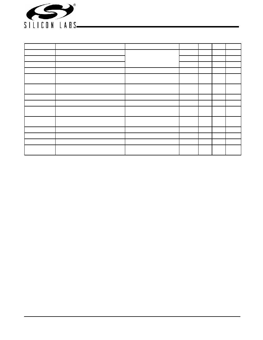
Parameter
Description
Conditions
Min.
Typ.
Max.
Unit
fCLK
Operating Clock Frequency
AVDD, VDD = 2.5V ± 0.2V
60
170
MHz
tDC
Input Clock Duty Cycle[13]
40
60
%
tlock
Maximum PLL lock Time
100
s
tR/tF
Output Clocks Slew Rate
20% to 80% of VOD
1
2
V/ns
tpZL, tpZH
Output Enable Time[14]
(all outputs)
3
ns
tpLZ, tpHZ
Output Disable Time[14]
(all outputs)
3
ns
tCCJ
Cycle to Cycle Jitter
f > 66 MHz
–100
100
ps
tjit(h-per)
Half-period jitter [15]
f > 66 MHz
–100
100
ps
tPLH
Low-to-High Propagation Delay,
CLKINT to YT[0:9]
1.5
3.5
6ns
tPHL
High-to-Low Propagation Delay,
CLKINT to YT[0:9]
1.5
3.5
6ns
tSK(0)
Any Output to Any Output Skew[16]
100
ps
tPHASE
Phase Error[16]
–150
150
ps
tJITT(PHASE)
Phase Error Jitter
f > 66 MHz
–50
50
ps
td(0)
Dynamic Phase Offset
CLKIN pins to FBIN pins at the
DUT[17]
30
140
ps
相关PDF资料 |
PDF描述 |
|---|---|
| V150A5H400B3 | CONVERTER MOD DC/DC 5V 400W |
| V110A36H400BF3 | CONVERTER MOD DC/DC 36V 400W |
| VE-JN3-MY | CONVERTER MOD DC/DC 24V 50W |
| VE-JN2-MY | CONVERTER MOD DC/DC 15V 50W |
| VE-JN1-MY | CONVERTER MOD DC/DC 12V 50W |
相关代理商/技术参数 |
参数描述 |
|---|---|
| CY2SSTV850ZCT | 功能描述:时钟缓冲器 2.5V 170MHz 1:10 Diff DDR PLL+I2C RoHS:否 制造商:Texas Instruments 输出端数量:5 最大输入频率:40 MHz 传播延迟(最大值): 电源电压-最大:3.45 V 电源电压-最小:2.375 V 最大功率耗散: 最大工作温度:+ 85 C 最小工作温度:- 40 C 封装 / 箱体:LLP-24 封装:Reel |
| CY2SSTV850ZI | 功能描述:时钟缓冲器 DDR1 Clock PLL RoHS:否 制造商:Texas Instruments 输出端数量:5 最大输入频率:40 MHz 传播延迟(最大值): 电源电压-最大:3.45 V 电源电压-最小:2.375 V 最大功率耗散: 最大工作温度:+ 85 C 最小工作温度:- 40 C 封装 / 箱体:LLP-24 封装:Reel |
| CY2SSTV850ZIT | 功能描述:时钟缓冲器 DDR1 Clock PLL RoHS:否 制造商:Texas Instruments 输出端数量:5 最大输入频率:40 MHz 传播延迟(最大值): 电源电压-最大:3.45 V 电源电压-最小:2.375 V 最大功率耗散: 最大工作温度:+ 85 C 最小工作温度:- 40 C 封装 / 箱体:LLP-24 封装:Reel |
| CY2SSTV855 | 制造商:CYPRESS 制造商全称:Cypress Semiconductor 功能描述:Differential Clock Buffer/Driver |
| CY2SSTV855_06 | 制造商:CYPRESS 制造商全称:Cypress Semiconductor 功能描述:Differential Clock Buffer/Driver |
发布紧急采购,3分钟左右您将得到回复。