- 您现在的位置:买卖IC网 > PDF目录8706 > CY2SSTV850ZC (Silicon Laboratories Inc)IC PLL BUF/DRIV I2C 1:10 48TSSOP PDF资料下载
参数资料
| 型号: | CY2SSTV850ZC |
| 厂商: | Silicon Laboratories Inc |
| 文件页数: | 3/9页 |
| 文件大小: | 0K |
| 描述: | IC PLL BUF/DRIV I2C 1:10 48TSSOP |
| 标准包装: | 39 |
| 类型: | * |
| PLL: | 带旁路 |
| 输入: | 时钟 |
| 输出: | 时钟 |
| 电路数: | 1 |
| 比率 - 输入:输出: | 1:10 |
| 差分 - 输入:输出: | 是/是 |
| 频率 - 最大: | 170MHz |
| 除法器/乘法器: | 无/无 |
| 电源电压: | 2.375 V ~ 3.465 V |
| 工作温度: | 0°C ~ 70°C |
| 安装类型: | * |
| 封装/外壳: | * |
| 供应商设备封装: | * |
| 包装: | * |
CY2SSTV850
......................... Document #: 38-07457 Rev. *A Page 3 of 9
Power Management
The
individual
output
enable/disable
control
of
the
CY2SSTV850 allows the user to implement unique power
management
schemes
into
the
design.
Outputs
are
three-stated when disabled through the two-line interface as
individual bits are set low in Byte 0 and Byte 1 registers. The
feedback output pair (FBOUTT, FBOUTC) cannot be disabled
via two-line serial bus. The enabling and disabling of individual
outputs is done in such a manner as to eliminate the possibility
of partial “runt” clocks.
Zero-delay Buffer
When used as a zero-delay buffer the CY2SSTV850 will likely
be in a nested clock tree application. For these applications
the CY2SSTV850 offers a differential clock input pair as a PLL
reference. The CY2SSTV850 then can lock onto the reference
and translate with near zero delay to low-skew outputs. For
normal operation, the external feedback input, FBINT, is
connected to the feedback output, FBOUTT. By connecting
the feedback output to the feedback input the propagation
delay through the device is eliminated. The PLL works to align
the output edge with the input reference edge thus producing
a near zero delay. The reference frequency affects the static
phase offset of the PLL and thus the relative delay between
the inputs and outputs.
When AVDD is strapped low, the PLL is turned off and
bypassed for test purposes.
Serial Control Registers
Following the acknowledge of the Address Byte, two additional
bytes must be sent:
“Command Code” byte, and “Byte Count” byte.
2 Line Serial Interface
Note:
3. Each output pair can be three-stated via the two-line serial interface.
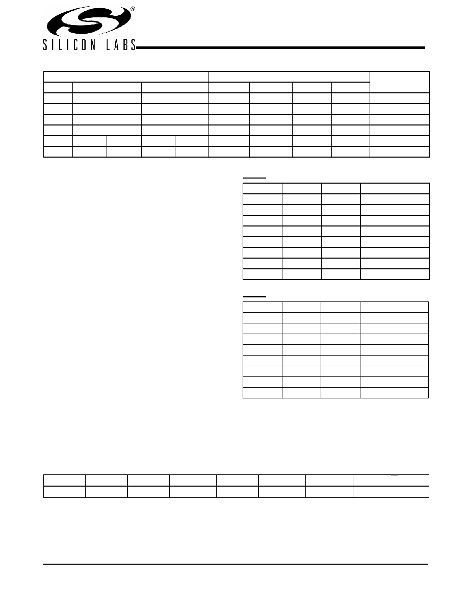
Function Table
Inputs
Outputs
PLL
AVDD
CLKINT
CLKINC
YT(0:9)[3]
YC(0:9)[3]
FBOUTT
FBOUTC
GND
L
H
L
H
L
H
BYPASSED/OFF
GND
H
L
H
L
H
L
BYPASSED/OFF
2.5V
L
H
L
H
L
H
On
2.5V
H
L
H
L
H
L
On
Nom
Design
Nom
Design
2.5V
<20 MHz
<30 MHZ <20 MHz <30 MHz
Hi-Z
Off
Byte0: Output Register (1 = Enable, 0 = Disable)
Bit
@Pup
Pin#
Description
71
3, 2
YT0, YC0
61
5, 6
YT1, YC1
51
10, 9
YT2, YC2
4
1
20, 19
YT3, YC3
3
1
22, 23
YT4, YC4
2
1
46, 47
YT5, YC5
1
44, 43
YT6, YC6
0
1
39, 40
YT7, YC7
Byte1: Output Register (1 = Enable, 0 = Disable)
Bit
@Pup
Pin#
Description
7
1
29, 30
YT8, YC8
6
1
27, 26
YT9, YC9
50
Reserved
40
Reserved
30
Reserved
20
Reserved
10
Reserved
00
Reserved
2-Line Serial Interface Slave Address
A7
A6
A5
A4
A3
A2
A1
R/W
1
0100
1
0
Writing to the device is accomplished by sequentially sending the device address D2H, the dummy bytes (command code and
the number of bytes), and the data bytes. This sequence is illustrated in the following tables.
相关PDF资料 |
PDF描述 |
|---|---|
| V150A5H400B3 | CONVERTER MOD DC/DC 5V 400W |
| V110A36H400BF3 | CONVERTER MOD DC/DC 36V 400W |
| VE-JN3-MY | CONVERTER MOD DC/DC 24V 50W |
| VE-JN2-MY | CONVERTER MOD DC/DC 15V 50W |
| VE-JN1-MY | CONVERTER MOD DC/DC 12V 50W |
相关代理商/技术参数 |
参数描述 |
|---|---|
| CY2SSTV850ZCT | 功能描述:时钟缓冲器 2.5V 170MHz 1:10 Diff DDR PLL+I2C RoHS:否 制造商:Texas Instruments 输出端数量:5 最大输入频率:40 MHz 传播延迟(最大值): 电源电压-最大:3.45 V 电源电压-最小:2.375 V 最大功率耗散: 最大工作温度:+ 85 C 最小工作温度:- 40 C 封装 / 箱体:LLP-24 封装:Reel |
| CY2SSTV850ZI | 功能描述:时钟缓冲器 DDR1 Clock PLL RoHS:否 制造商:Texas Instruments 输出端数量:5 最大输入频率:40 MHz 传播延迟(最大值): 电源电压-最大:3.45 V 电源电压-最小:2.375 V 最大功率耗散: 最大工作温度:+ 85 C 最小工作温度:- 40 C 封装 / 箱体:LLP-24 封装:Reel |
| CY2SSTV850ZIT | 功能描述:时钟缓冲器 DDR1 Clock PLL RoHS:否 制造商:Texas Instruments 输出端数量:5 最大输入频率:40 MHz 传播延迟(最大值): 电源电压-最大:3.45 V 电源电压-最小:2.375 V 最大功率耗散: 最大工作温度:+ 85 C 最小工作温度:- 40 C 封装 / 箱体:LLP-24 封装:Reel |
| CY2SSTV855 | 制造商:CYPRESS 制造商全称:Cypress Semiconductor 功能描述:Differential Clock Buffer/Driver |
| CY2SSTV855_06 | 制造商:CYPRESS 制造商全称:Cypress Semiconductor 功能描述:Differential Clock Buffer/Driver |
发布紧急采购,3分钟左右您将得到回复。