- 您现在的位置:买卖IC网 > PDF目录9591 > CY2SSTV857ZXC-32T (Silicon Laboratories Inc)IC CLK DDR266/333BUF1:10 48TSSOP PDF资料下载
参数资料
| 型号: | CY2SSTV857ZXC-32T |
| 厂商: | Silicon Laboratories Inc |
| 文件页数: | 3/8页 |
| 文件大小: | 0K |
| 描述: | IC CLK DDR266/333BUF1:10 48TSSOP |
| 标准包装: | 2,000 |
| 系列: | * |
| 类型: | * |
| PLL: | * |
| 主要目的: | * |
| 输入: | * |
| 输出: | * |
| 电路数: | * |
| 比率 - 输入:输出: | * |
| 差分 - 输入:输出: | * |
| 频率 - 最大: | * |
| 电源电压: | * |
| 工作温度: | * |
| 安装类型: | * |
| 封装/外壳: | * |
| 供应商设备封装: | * |
| 包装: | * |
CY2SSTV857
.......................... Document #: 38-07557 Rev. *E Page 3 of 8
Zero Delay Buffer
When used as a zero delay buffer the CY2SSTV857-32 will
likely be in a nested clock tree application. For these applica-
tions, the CY2SSTV857-32 offers a differential clock input pair
as a PLL reference. The CY2SSTV857-32 then can lock onto
the reference and translate with near zero delay to low-skew
outputs. For normal operation, the external feedback input,
FBIN, is connected to the feedback output, FBOUT. By
connecting the feedback output to the feedback input the
propagation delay through the device is eliminated. The PLL
works to align the output edge with the input reference edge
thus producing a near zero delay. The reference frequency
affects the static phase offset of the PLL and thus the relative
delay between the inputs and outputs.
When VDDA is strapped LOW, the PLL is turned off and
bypassed for test purposes.
Power Management
Output enable/disable control of the CY2SSTV857-32 allows
the user to implement power management schemes into the
design. Outputs are three-stated/disabled when PD# is
asserted LOW (see Table 1).
Table 1. Function Table
Inputs
Outputs
PLL
AVDD
PD#
CLK
CLK#
Y
Y#
FBOUT
FBOUT#
GND
H
L
H
L
H
L
H
BYPASSED/OFF
GND
H
L
H
L
H
L
BYPASSED/OFF
XL
L
H
Z
ZZ
Off
XL
H
L
Z
ZZ
OFF
2.6V
H
L
H
L
H
L
H
On
2.6V
H
L
H
L
H
L
On
2.6V
H
< 20 MHz
Hi-Z
HI-Z
Off
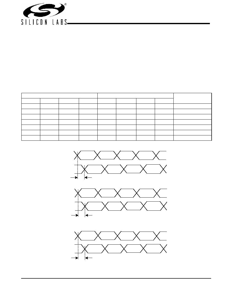
CLKIN
t
(phase error)
FBIN
FBOUT
t
sk(o)
Yx
t
sk(o)
Figure 1. Phase Error and Skew Waveforms
相关PDF资料 |
PDF描述 |
|---|---|
| ICS9DB202CFLFT | IC JITTER ATTENUATOR 20-SSOP |
| MS3128F16-26P | CONN RCPT 26POS WALL MNT W/PINS |
| MS3128F14-12S | CONN RCPT 12POS WALL MNT W/SCKT |
| SL28504BZI-2T | IC CLOCK GEN EAGLELAKE 56TSSOP |
| ICL3238CA-T | IC 5DRVR/3RCVR RS232 3V 28-SSOP |
相关代理商/技术参数 |
参数描述 |
|---|---|
| CY2SSTV857ZXI-27 | 功能描述:时钟缓冲器 2.5V 60-200MHz 1:10 Diff DDR266/333 B/D RoHS:否 制造商:Texas Instruments 输出端数量:5 最大输入频率:40 MHz 传播延迟(最大值): 电源电压-最大:3.45 V 电源电压-最小:2.375 V 最大功率耗散: 最大工作温度:+ 85 C 最小工作温度:- 40 C 封装 / 箱体:LLP-24 封装:Reel |
| CY2SSTV857ZXI-27T | 功能描述:时钟缓冲器 2.5V 60-200MHz 1:10 Diff DDR266/333 B/D RoHS:否 制造商:Texas Instruments 输出端数量:5 最大输入频率:40 MHz 传播延迟(最大值): 电源电压-最大:3.45 V 电源电压-最小:2.375 V 最大功率耗散: 最大工作温度:+ 85 C 最小工作温度:- 40 C 封装 / 箱体:LLP-24 封装:Reel |
| CY2SSTV857ZXI-32 | 功能描述:时钟缓冲器 2.5V 60-200MHz 1:10 Diff DDR266/333 B/D RoHS:否 制造商:Texas Instruments 输出端数量:5 最大输入频率:40 MHz 传播延迟(最大值): 电源电压-最大:3.45 V 电源电压-最小:2.375 V 最大功率耗散: 最大工作温度:+ 85 C 最小工作温度:- 40 C 封装 / 箱体:LLP-24 封装:Reel |
| CY2SSTV857ZXI-32T | 功能描述:时钟缓冲器 2.5V 60-200MHz 1:10 Diff DDR266/333 B/D RoHS:否 制造商:Texas Instruments 输出端数量:5 最大输入频率:40 MHz 传播延迟(最大值): 电源电压-最大:3.45 V 电源电压-最小:2.375 V 最大功率耗散: 最大工作温度:+ 85 C 最小工作温度:- 40 C 封装 / 箱体:LLP-24 封装:Reel |
| CY2V012FLXCT | 制造商:Cypress Semiconductor 功能描述: |
发布紧急采购,3分钟左右您将得到回复。