- 您现在的位置:买卖IC网 > PDF目录19907 > XCF01SVOG20C (Xilinx Inc)IC PROM SRL FOR 1M GATE 20-TSSOP PDF资料下载
参数资料
| 型号: | XCF01SVOG20C |
| 厂商: | Xilinx Inc |
| 文件页数: | 3/35页 |
| 文件大小: | 0K |
| 描述: | IC PROM SRL FOR 1M GATE 20-TSSOP |
| 标准包装: | 74 |
| 可编程类型: | 系统内可编程 |
| 存储容量: | 1Mb |
| 电源电压: | 3 V ~ 3.6 V |
| 工作温度: | -40°C ~ 85°C |
| 封装/外壳: | 20-TSSOP(0.173",4.40mm 宽) |
| 供应商设备封装: | 20-TSSOP |
| 包装: | 管件 |
| 产品目录页面: | 601 (CN2011-ZH PDF) |
| 其它名称: | 122-1286-5 |
第1页第2页当前第3页第4页第5页第6页第7页第8页第9页第10页第11页第12页第13页第14页第15页第16页第17页第18页第19页第20页第21页第22页第23页第24页第25页第26页第27页第28页第29页第30页第31页第32页第33页第34页第35页
Platform Flash In-System Programmable Configuration PROMs
DS123 (v2.18) May 19, 2010
Product Specification
11
R
Reset and Power-On Reset Activation
At power up, the device requires the VCCINT power supply to
monotonically rise to the nominal operating voltage within
the specified VCCINT rise time. If the power supply cannot
meet this requirement, then the device might not perform
power-on reset properly. During the power-up sequence,
OE/RESET is held Low by the PROM. Once the required
supplies have reached their respective POR (Power On
Reset) thresholds, the OE/RESET release is delayed (TOER
minimum) to allow more margin for the power supplies to
stabilize before initiating configuration. The OE/RESET pin
is connected to an external 4.7 k
Ω pull-up resistor and also
to the target FPGA's INIT pin. For systems utilizing slow-
rising power supplies, an additional power monitoring circuit
can be used to delay the target configuration until the
system power reaches minimum operating voltages by
holding the OE/RESET pin Low. When OE/RESET is
released, the FPGA’s INIT pin is pulled High allowing the
FPGA's configuration sequence to begin. If the power drops
below the power-down threshold (VCCPD), the PROM resets
and OE/RESET is again held Low until the after the POR
threshold is reached. OE/RESET polarity is not
programmable. These power-up requirements are shown
graphically in Figure 6.
For a fully powered Platform Flash PROM, a reset occurs
whenever OE/RESET is asserted (Low) or CE is deasserted
(High). The address counter is reset, CEO is driven High, and
the remaining outputs are placed in a high-impedance state.
Note:
1.
The XCFxxS PROM only requires VCCINT to rise above
its POR threshold before releasing OE/RESET.
2.
The XCFxxP PROM requires both VCCINT to rise above its
POR threshold and for VCCO to reach the recommended
operating voltage level before releasing OE/RESET.
I/O Input Voltage Tolerance and Power Sequencing
The I/Os on each re-programmable Platform Flash PROM
are fully 3.3V-tolerant. This allows 3V CMOS signals to
connect directly to the inputs without damage. The core
power supply (VCCINT), JTAG pin power supply (VCCJ),
output power supply (VCCO), and external 3V CMOS I/O
signals can be applied in any order.
Additionally, for the XCFxxS PROM only, when VCCO is
supplied at 2.5V or 3.3V and VCCINT is supplied at 3.3V, the
I/Os are 5V-tolerant. This allows 5V CMOS signals to
connect directly to the inputs on a powered XCFxxS PROM
without damage. Failure to power the PROM correctly while
supplying a 5V input signal can result in damage to the
XCFxxS device.
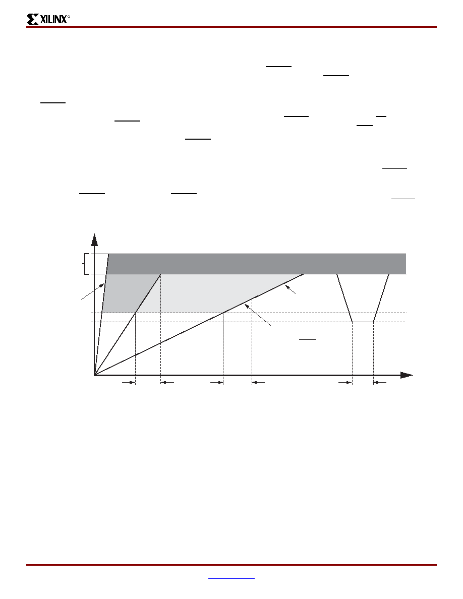
X-Ref Target - Figure 6
Figure 6: Platform Flash PROM Power-Up Requirements
TOER
VCCINT
VCCPOR
VCCPD
200 s ramp
50 ms ramp
TOER
TRST
TIME (ms)
A slow-ramping VCCINT supply may still
be below the minimum operating
voltage when OE/RESET is released.
In this case, the configuration
sequence must be delayed until both
VCCINT and VCCO have reached their
recommended operating conditions.
Recommended Operating Range
Delay or Restart
Configuration
ds123_21_103103
相关PDF资料 |
PDF描述 |
|---|---|
| EEM10DRYF | CONN EDGECARD 20POS DIP .156 SLD |
| V48C8H100BG | CONVERTER MOD DC/DC 8V 100W |
| EPC16UC88N | IC CONFIG DEVICE 16MBIT 88-UBGA |
| LTC4301IDD#TR | IC BUFFER BUS HOTSWAP 2WR 8DFN |
| AGM22DTBH | CONN EDGECARD 44POS R/A .156 SLD |
相关代理商/技术参数 |
参数描述 |
|---|---|
| CY2SSTV857ZXI-32T | 功能描述:时钟缓冲器 2.5V 60-200MHz 1:10 Diff DDR266/333 B/D RoHS:否 制造商:Texas Instruments 输出端数量:5 最大输入频率:40 MHz 传播延迟(最大值): 电源电压-最大:3.45 V 电源电压-最小:2.375 V 最大功率耗散: 最大工作温度:+ 85 C 最小工作温度:- 40 C 封装 / 箱体:LLP-24 封装:Reel |
| CY2V012FLXCT | 制造商:Cypress Semiconductor 功能描述: |
| CY2V013FLXCT | 功能描述:锁相环 - PLL IC XTAL OSC VOLT RoHS:否 制造商:Silicon Labs 类型:PLL Clock Multiplier 电路数量:1 最大输入频率:710 MHz 最小输入频率:0.002 MHz 输出频率范围:0.002 MHz to 808 MHz 电源电压-最大:3.63 V 电源电压-最小:1.71 V 最大工作温度:+ 85 C 最小工作温度:- 40 C 封装 / 箱体:QFN-36 封装:Tray |
| CY2V013FLXIT | 功能描述:锁相环 - PLL FleXo HiPerf ClkGen RoHS:否 制造商:Silicon Labs 类型:PLL Clock Multiplier 电路数量:1 最大输入频率:710 MHz 最小输入频率:0.002 MHz 输出频率范围:0.002 MHz to 808 MHz 电源电压-最大:3.63 V 电源电压-最小:1.71 V 最大工作温度:+ 85 C 最小工作温度:- 40 C 封装 / 箱体:QFN-36 封装:Tray |
| CY2V014FLXCT | 功能描述:锁相环 - PLL IC XTAL OSC VOLT RoHS:否 制造商:Silicon Labs 类型:PLL Clock Multiplier 电路数量:1 最大输入频率:710 MHz 最小输入频率:0.002 MHz 输出频率范围:0.002 MHz to 808 MHz 电源电压-最大:3.63 V 电源电压-最小:1.71 V 最大工作温度:+ 85 C 最小工作温度:- 40 C 封装 / 箱体:QFN-36 封装:Tray |
发布紧急采购,3分钟左右您将得到回复。