- 您现在的位置:买卖IC网 > PDF目录19907 > XCF01SVOG20C (Xilinx Inc)IC PROM SRL FOR 1M GATE 20-TSSOP PDF资料下载
参数资料
| 型号: | XCF01SVOG20C |
| 厂商: | Xilinx Inc |
| 文件页数: | 19/35页 |
| 文件大小: | 0K |
| 描述: | IC PROM SRL FOR 1M GATE 20-TSSOP |
| 标准包装: | 74 |
| 可编程类型: | 系统内可编程 |
| 存储容量: | 1Mb |
| 电源电压: | 3 V ~ 3.6 V |
| 工作温度: | -40°C ~ 85°C |
| 封装/外壳: | 20-TSSOP(0.173",4.40mm 宽) |
| 供应商设备封装: | 20-TSSOP |
| 包装: | 管件 |
| 产品目录页面: | 601 (CN2011-ZH PDF) |
| 其它名称: | 122-1286-5 |
第1页第2页第3页第4页第5页第6页第7页第8页第9页第10页第11页第12页第13页第14页第15页第16页第17页第18页当前第19页第20页第21页第22页第23页第24页第25页第26页第27页第28页第29页第30页第31页第32页第33页第34页第35页
Platform Flash In-System Programmable Configuration PROMs
DS123 (v2.18) May 19, 2010
Product Specification
26
R
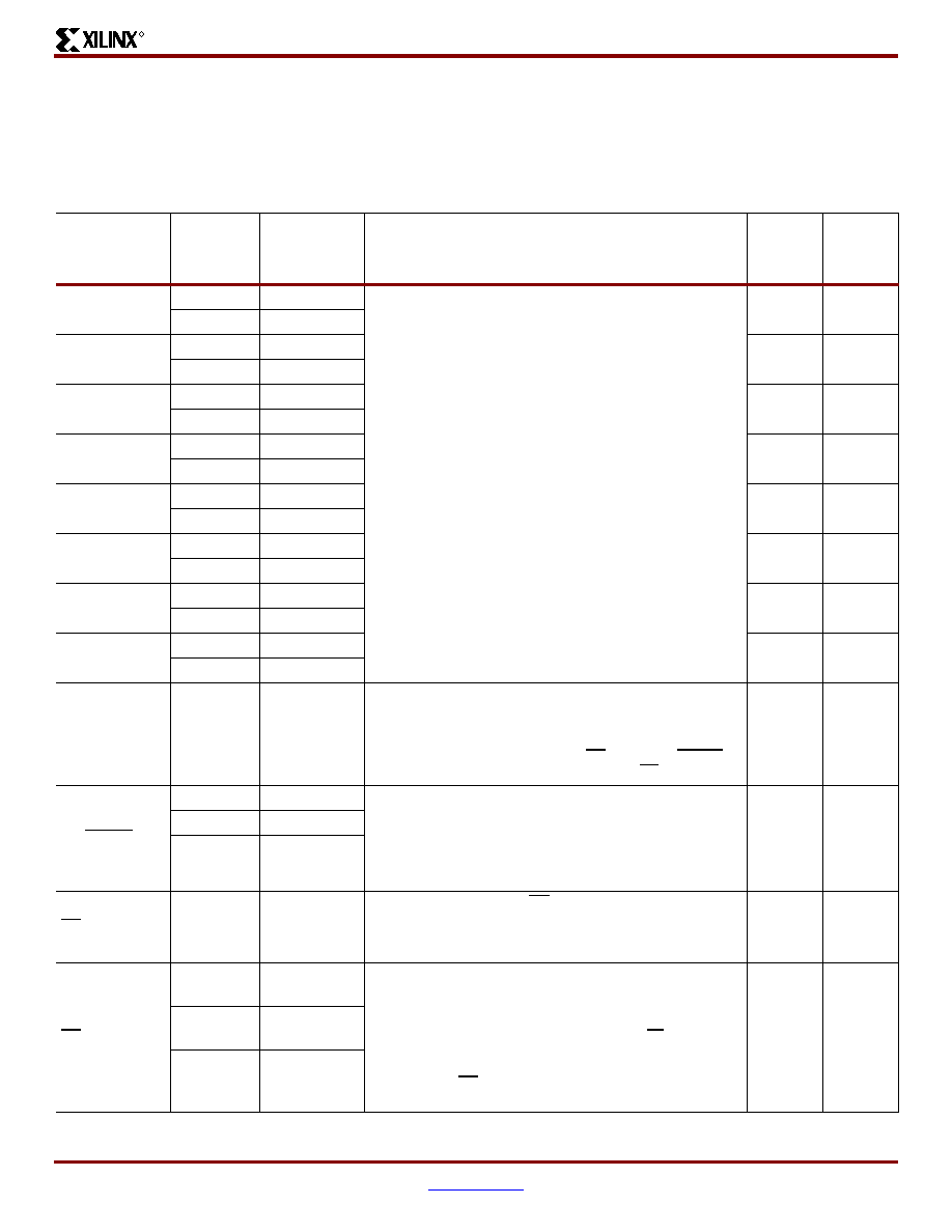
XCFxxP Pinouts and Pin Descriptions
XCFxxP VO48/VOG48 and FS48/FSG48 Pin Names and Descriptions
Table 13 provides a list of the pin names and descriptions for the XCFxxP 48-pin VO48/VOG48 and 48-pin
FS48/FSG48 packages.
Table 13: XCFxxP Pin Names and Descriptions (VO48/VOG48 and FS48/FSG48)
Pin Name
Boundary-
Scan Order
Boundary-
Scan
Function
Pin Description
48-pin
TSOP
(VO48/
VOG48)
48-pin
TFBGA
(FS48/
FSG48)
D0
28
Data Out
D0 is the DATA output pin to provide data for configuring an
FPGA in serial mode.
D0-D7 are the DATA output pins to provide parallel data for
configuring a Xilinx FPGA in SelectMap (parallel) mode.
The D0 output is set to a high-impedance state during ISPEN
(when not clamped).
The D1-D7 outputs are set to a high-impedance state during
ISPEN (when not clamped) and when serial mode is selected
for configuration. The D1-D7 pins can be left unconnected
when the PROM is used in serial mode.
28
H6
27
Output Enable
D1
26
Data Out
29
H5
25
Output Enable
D2
24
Data Out
32
E5
23
Output Enable
D3
22
Data Out
33
D5
21
Output Enable
D4
20
Data Out
43
C5
19
Output Enable
D5
18
Data Out
44
B5
17
Output Enable
D6
16
Data Out
47
A5
15
Output Enable
D7
14
Data Out
48
A6
13
Output Enable
CLK
01
Data In
Configuration Clock Input. An internal programmable control bit
selects between the internal oscillator and the CLK input pin as
the clock source to control the configuration sequence. Each
rising edge on the CLK input increments the internal address
counter if the CLK input is selected, CE is Low, OE/RESET is
High, BUSY is Low (parallel mode only), and CF is High.
12
B3
OE/RESET
04
Data In
Output Enable/Reset (Open-Drain I/O).
When Low, this input holds the address counter reset and the
DATA and CLKOUT outputs are placed in a high-impedance
state. This is a bidirectional open-drain pin that is held Low
while the PROM completes the internal power-on reset
sequence. Polarity is not programmable.
11
A3
03
Data Out
02
Output Enable
CE
00
Data In
Chip Enable Input. When CE is High, the device is put into
low-power standby mode, the address counter is reset, and
the DATA and CLKOUT outputs are placed in a high-
impedance state.
13
B4
CF
11
Data In
Configuration Pulse (Open-Drain I/O). As an output, this pin
allows the JTAG CONFIG instruction to initiate FPGA
configuration without powering down the FPGA. This is an
open-drain signal that is pulsed Low by the JTAG CONFIG
command. As an input, on the rising edge of CF, the current
design revision selection is sampled and the internal address
counter is reset to the start address for the selected revision.
If unused, the CF pin must be pulled High using an external
4.7 k
Ω pull-up to V
CCO.
6D1
10
Data Out
09
Output Enable
相关PDF资料 |
PDF描述 |
|---|---|
| EEM10DRYF | CONN EDGECARD 20POS DIP .156 SLD |
| V48C8H100BG | CONVERTER MOD DC/DC 8V 100W |
| EPC16UC88N | IC CONFIG DEVICE 16MBIT 88-UBGA |
| LTC4301IDD#TR | IC BUFFER BUS HOTSWAP 2WR 8DFN |
| AGM22DTBH | CONN EDGECARD 44POS R/A .156 SLD |
相关代理商/技术参数 |
参数描述 |
|---|---|
| XCF01SVOG20C0100 | 制造商:Xilinx 功能描述:XLXXCF01SVOG20C0100 IC SYSTEM GATE |
| XCF01SVOG20C0936 | 制造商:Xilinx 功能描述:XLXXCF01SVOG20C0936 IC SYSTEM GATE |
| XCF01SVOG48 | 制造商:XILINX 制造商全称:XILINX 功能描述:Platform Flash In-System Programmable Configuration PROMS |
| XCF01SX | 制造商:XILINX 制造商全称:XILINX 功能描述:Platform Flash In-System Programmable Configuration PROMS |
| XCF02S | 制造商:XILINX 制造商全称:XILINX 功能描述:Platform Flash In-System Programmable Configuration PROMs |
发布紧急采购,3分钟左右您将得到回复。