- 您现在的位置:买卖IC网 > PDF目录19907 > XCF01SVOG20C (Xilinx Inc)IC PROM SRL FOR 1M GATE 20-TSSOP PDF资料下载
参数资料
| 型号: | XCF01SVOG20C |
| 厂商: | Xilinx Inc |
| 文件页数: | 20/35页 |
| 文件大小: | 0K |
| 描述: | IC PROM SRL FOR 1M GATE 20-TSSOP |
| 标准包装: | 74 |
| 可编程类型: | 系统内可编程 |
| 存储容量: | 1Mb |
| 电源电压: | 3 V ~ 3.6 V |
| 工作温度: | -40°C ~ 85°C |
| 封装/外壳: | 20-TSSOP(0.173",4.40mm 宽) |
| 供应商设备封装: | 20-TSSOP |
| 包装: | 管件 |
| 产品目录页面: | 601 (CN2011-ZH PDF) |
| 其它名称: | 122-1286-5 |
第1页第2页第3页第4页第5页第6页第7页第8页第9页第10页第11页第12页第13页第14页第15页第16页第17页第18页第19页当前第20页第21页第22页第23页第24页第25页第26页第27页第28页第29页第30页第31页第32页第33页第34页第35页
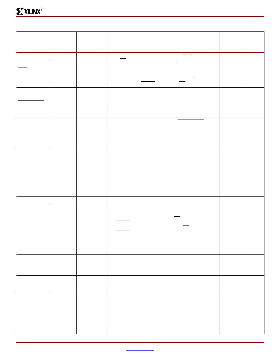
Platform Flash In-System Programmable Configuration PROMs
DS123 (v2.18) May 19, 2010
Product Specification
27
R
CEO
06
Data Out
Chip Enable Output. Chip Enable Output (CEO) is connected
to the CE input of the next PROM in the chain. This output is
Low when CE is Low and OE/RESET input is High, AND the
internal address counter has been incremented beyond its
Terminal Count (TC) value or the PROM does not contain any
blocks that correspond to the selected revision. CEO returns
to High when OE/RESET goes Low or CE goes High.
10
D2
05
Output Enable
EN_EXT_SEL
31
Data In
Enable External Selection Input. When this pin is Low, design
revision selection is controlled by the Revision Select pins.
When this pin is High, design revision selection is controlled
by the internal programmable Revision Select control bits.
EN_EXT_SEL has an internal 50 k
Ω resistive pull-up to
VCCO to provide a logic 1 to the device if the pin is not driven.
25
H4
REV_SEL0
30
Data In
Revision Select[1:0] Inputs. When the EN_EXT_SEL is Low,
the Revision Select pins are used to select the design
revision to be enabled, overriding the internal programmable
Revision Select control bits. The Revision Select[1:0] inputs
have an internal 50 k
Ω resistive pull-up to V
CCO to provide a
logic 1 to the device if the pins are not driven.
26
G3
REV_SEL1
29
Data In
27
G4
BUSY
12
Data In
Busy Input. The BUSY input is enabled when parallel mode
is selected for configuration. When BUSY is High, the internal
address counter stops incrementing and the current data
remains on the data pins. On the first rising edge of CLK after
BUSY transitions from High to Low, the data for the next
address is driven on the data pins. When serial mode or
decompression is enabled during device programming, the
BUSY input is disabled. BUSY has an internal 50 k
Ω resistive
pull-down to GND to provide a logic 0 to the device if the pin
is not driven.
5C1
CLKOUT
08
Data Out
Configuration Clock Output. An internal Programmable
control bit enables the CLKOUT signal, which is sourced from
either the internal oscillator or the CLK input pin. Each rising
edge of the selected clock source increments the internal
address counter if data is available, CE is Low, and
OE/RESET is High. Output data is available on the rising
edge of CLKOUT. CLKOUT is disabled if CE is High or
OE/RESET is Low. If decompression is enabled, CLKOUT is
parked High when decompressed data is not ready. When
CLKOUT is disabled, the CLKOUT pin is put into a high-Z
state. If CLKOUT is used, then it must be pulled High
externally using a 4.7 k
Ω pull-up to V
CCO.
9C2
07
Output Enable
TMS
–
Mode Select
JTAG Mode Select Input. The state of TMS on the rising edge
of TCK determines the state transitions at the Test Access Port
(TAP) controller. TMS has an internal 50 k
Ω resistive pull-up to
VCCJ to provide a logic 1 to the device if the pin is not driven.
21
E2
TCK
–
Clock
JTAG Clock Input. This pin is the JTAG test clock. It
sequences the TAP controller and all the JTAG test and
programming electronics.
20
H3
TDI
–
Data In
JTAG Serial Data Input. This pin is the serial input to all JTAG
instruction and data registers. TDI has an internal 50 k
Ω
resistive pull-up to VCCJ to provide a logic 1 to the device if
the pin is not driven.
19
G1
TDO
–
Data Out
JTAG Serial Data Output. This pin is the serial output for all
JTAG instruction and data registers. TDO has an internal
50 k
Ω resistive pull-up to V
CCJ to provide a logic 1 to the
system if the pin is not driven.
22
E6
Table 13: XCFxxP Pin Names and Descriptions (VO48/VOG48 and FS48/FSG48) (Cont’d)
Pin Name
Boundary-
Scan Order
Boundary-
Scan
Function
Pin Description
48-pin
TSOP
(VO48/
VOG48)
48-pin
TFBGA
(FS48/
FSG48)
相关PDF资料 |
PDF描述 |
|---|---|
| EEM10DRYF | CONN EDGECARD 20POS DIP .156 SLD |
| V48C8H100BG | CONVERTER MOD DC/DC 8V 100W |
| EPC16UC88N | IC CONFIG DEVICE 16MBIT 88-UBGA |
| LTC4301IDD#TR | IC BUFFER BUS HOTSWAP 2WR 8DFN |
| AGM22DTBH | CONN EDGECARD 44POS R/A .156 SLD |
相关代理商/技术参数 |
参数描述 |
|---|---|
| XCF01SVOG20C0100 | 制造商:Xilinx 功能描述:XLXXCF01SVOG20C0100 IC SYSTEM GATE |
| XCF01SVOG20C0936 | 制造商:Xilinx 功能描述:XLXXCF01SVOG20C0936 IC SYSTEM GATE |
| XCF01SVOG48 | 制造商:XILINX 制造商全称:XILINX 功能描述:Platform Flash In-System Programmable Configuration PROMS |
| XCF01SX | 制造商:XILINX 制造商全称:XILINX 功能描述:Platform Flash In-System Programmable Configuration PROMS |
| XCF02S | 制造商:XILINX 制造商全称:XILINX 功能描述:Platform Flash In-System Programmable Configuration PROMs |
发布紧急采购,3分钟左右您将得到回复。