- 您现在的位置:买卖IC网 > PDF目录170654 > DAC702LH (TEXAS INSTRUMENTS INC) PARALLEL, WORD INPUT LOADING, 4 us SETTLING TIME, 16-BIT DAC, CDIP24 PDF资料下载
参数资料
| 型号: | DAC702LH |
| 厂商: | TEXAS INSTRUMENTS INC |
| 元件分类: | DAC |
| 英文描述: | PARALLEL, WORD INPUT LOADING, 4 us SETTLING TIME, 16-BIT DAC, CDIP24 |
| 封装: | HERMETIC SEALED, CERAMIC, DIP-24 |
| 文件页数: | 11/12页 |
| 文件大小: | 302K |
| 代理商: | DAC702LH |
8
DAC701, 702, 703
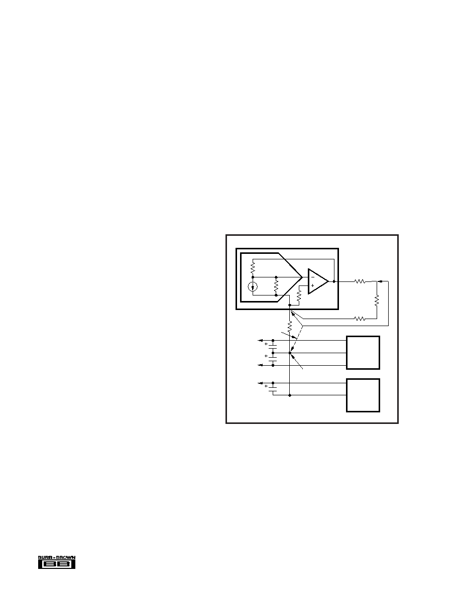
In many applications it is impractical to sense the output
voltage at the output pin. Sensing the output voltage at the
system ground point is permissible with the DAC700 family
because the D/A converter is designed to have a constant
return current of approximately 2mA flowing from Com-
mon. The variation in this current is under 20
A (with
changing input codes), therefore R4 can be as large as 3
without adversely affecting the linearity of the D/A con-
verter. The voltage drop across R4 (R4 x 2mA) appears as a
zero error and can be removed with the zero calibration
adjustment. This alternate sensing point (the system ground
point) is shown in Figures 6, 7, and 8.
Figures 7 and 8 show two methods of connecting the current
output models (DAC702) with external precision output op
amps. By sensing the output voltage at the load resistor (ie,
by connecting RF to the output of A1 at RL), the effect of R1
and R2 is greatly reduced. R1 will cause a gain error but is
independent of the value of RL and can be eliminated by
initial calibration adjustments. The effect of R2 is negligible
because it is inside the feedback loop of the output op amp
and is therefore greatly reduced by the loop gain.
Zero Adjustment
For unipolar (CSB) configurations, apply the digital input
code that produces zero voltage or zero current output and
adjust the zero potentiometer for zero output.
For bipolar (COB, CTC) configurations, apply the digital
input code that produces zero output voltage or current. See
Table II for corresponding codes and the Connection Dia-
gram for zero adjustment circuit connections. Zero calibra-
tion should be made before gain calibration.
Gain Adjustment
Apply the digital input that gives the maximum positive
output voltage. Adjust the gain potentiometer for this posi-
tive full scale voltage. See Table II for positive full scale
voltages and the Connection Diagram for gain adjustment
circuit connections.
INSTALLATION
CONSIDERATIONS
This D/A converter family is laser-trimmed to 14-bit linear-
ity. The design of the device makes the 16-bit resolution
available. If 16-bit resolution is not required, bit 15 and bit
16 should be connected to VDD through a single 1k
resistor.
Due to the extremely high resolution and linearity of the
D/A converter, system design problems such as grounding
and contact resistance become very important. For a 16-bit
converter with a 10V full-scale range, 1LSB is 153
V. With
a load current of 5mA, series wiring and connector resis-
tance of only 30m
will cause the output to be in error by
1LSB. To understand what this means in terms of a system
layout, the resistance of #23 wire is about 0.021
/ft. Ne-
glecting contact resistance, less than 18 inches of wire will
produce a 1LSB error in the analog output voltage!
In Figures 6, 7, and 8, lead and contact resistances are
represented by R1 through R5. As long as the load resistance
R
L is constant, R2 simply introduces a gain error and can be
removed during initial calibration. R3 is part of RL, if the
output voltage is sensed at Common, and therefore intro-
duces no error. If RL is variable, then R2 should be less than
R
L MIN/2
16 to reduce voltage drops due to wiring to less than
1LSB. For example, if RL MIN is 5k, then R2 should be less
than 0.08
. R
L should be located as close as possible to the
D/A converter for optimum performance. The effect of R4 is
negligible.
FIGURE 6. Output Circuit for Voltage Models.
A
1
R
DAC
4k
DAC701
5k
R
B
Common
V
OUT
R
2
*
R
L
R
3
Sense Output
+5VDC
Supply
±15VDC
Supply
+V
COM
–V
System Ground
Point
+V
COM
Alternate Ground
Sense Connection
R
4
To +V
CC
To –V
CC
To V
DD
1F
* R = 2k
(DAC701 and DAC703)
B
R
F
相关PDF资料 |
PDF描述 |
|---|---|
| DAC7545KUG4 | PARALLEL, WORD INPUT LOADING, 2 us SETTLING TIME, 12-BIT DAC, PDSO20 |
| DAC7545JP | PARALLEL, WORD INPUT LOADING, 2 us SETTLING TIME, 12-BIT DAC, PDIP20 |
| DAC7545KP | PARALLEL, WORD INPUT LOADING, 2 us SETTLING TIME, 12-BIT DAC, PDIP20 |
| DAC7554IDGSR | SERIAL INPUT LOADING, 5 us SETTLING TIME, 12-BIT DAC, PDSO10 |
| DAC7554IDGS | SERIAL INPUT LOADING, 5 us SETTLING TIME, 12-BIT DAC, PDSO10 |
相关代理商/技术参数 |
参数描述 |
|---|---|
| DAC702SH | 制造商:BB 制造商全称:BB 功能描述:Monolithic 16-Bit DIGITAL-TO-ANALOG CONVERTERS |
| DAC703 | 制造商:BB 制造商全称:BB 功能描述:Monolithic 16-Bit DIGITAL-TO-ANALOG CONVERTERS |
| DAC703B | 制造商:BB 制造商全称:BB 功能描述:Monolithic 16-Bit DIGITAL-TO-ANALOG CONVERTERS |
| DAC703BH | 制造商:BB 制造商全称:BB 功能描述:Monolithic 16-Bit DIGITAL-TO-ANALOG CONVERTERS |
| DAC703BH-BI | 制造商:BB 制造商全称:BB 功能描述:Monolithic 16-Bit DIGITAL-TO-ANALOG CONVERTERS |
发布紧急采购,3分钟左右您将得到回复。