- 您现在的位置:买卖IC网 > PDF目录170654 > DAC702LH (TEXAS INSTRUMENTS INC) PARALLEL, WORD INPUT LOADING, 4 us SETTLING TIME, 16-BIT DAC, CDIP24 PDF资料下载
参数资料
| 型号: | DAC702LH |
| 厂商: | TEXAS INSTRUMENTS INC |
| 元件分类: | DAC |
| 英文描述: | PARALLEL, WORD INPUT LOADING, 4 us SETTLING TIME, 16-BIT DAC, CDIP24 |
| 封装: | HERMETIC SEALED, CERAMIC, DIP-24 |
| 文件页数: | 9/12页 |
| 文件大小: | 302K |
| 代理商: | DAC702LH |
6
DAC701, 702, 703
DISCUSSION OF
SPECIFICATIONS
DIGITAL INPUT CODES
The DAC701/702/703 accept complementary digital
input codes in either binary format (CSB, unipolar or
COB, bipolar). The COB models DAC702/703 may be
connected by the user for either complementary offset
binary (COB) or complementary two’s complement (CTC)
codes (see Table I).
Zero Drift
Zero drift is a measure of the change in the output with
FFFFH (DAC701) applied to the digital inputs over the
specified temperature range. For the bipolar models, zero is
measured at 7FFFH (bipolar zero) applied to the digital
inputs. This code corresponds to zero volts (DAC703) or
zero milliamps (DAC702) at the analog output. The maxi-
mum change in offset at tMIN or tMAX is referenced to the
zero error at +25
°C and is divided by the temperature
change. This drift is expressed in parts per million of full
scale range per degree centigrade (ppm of FSR/
°C).
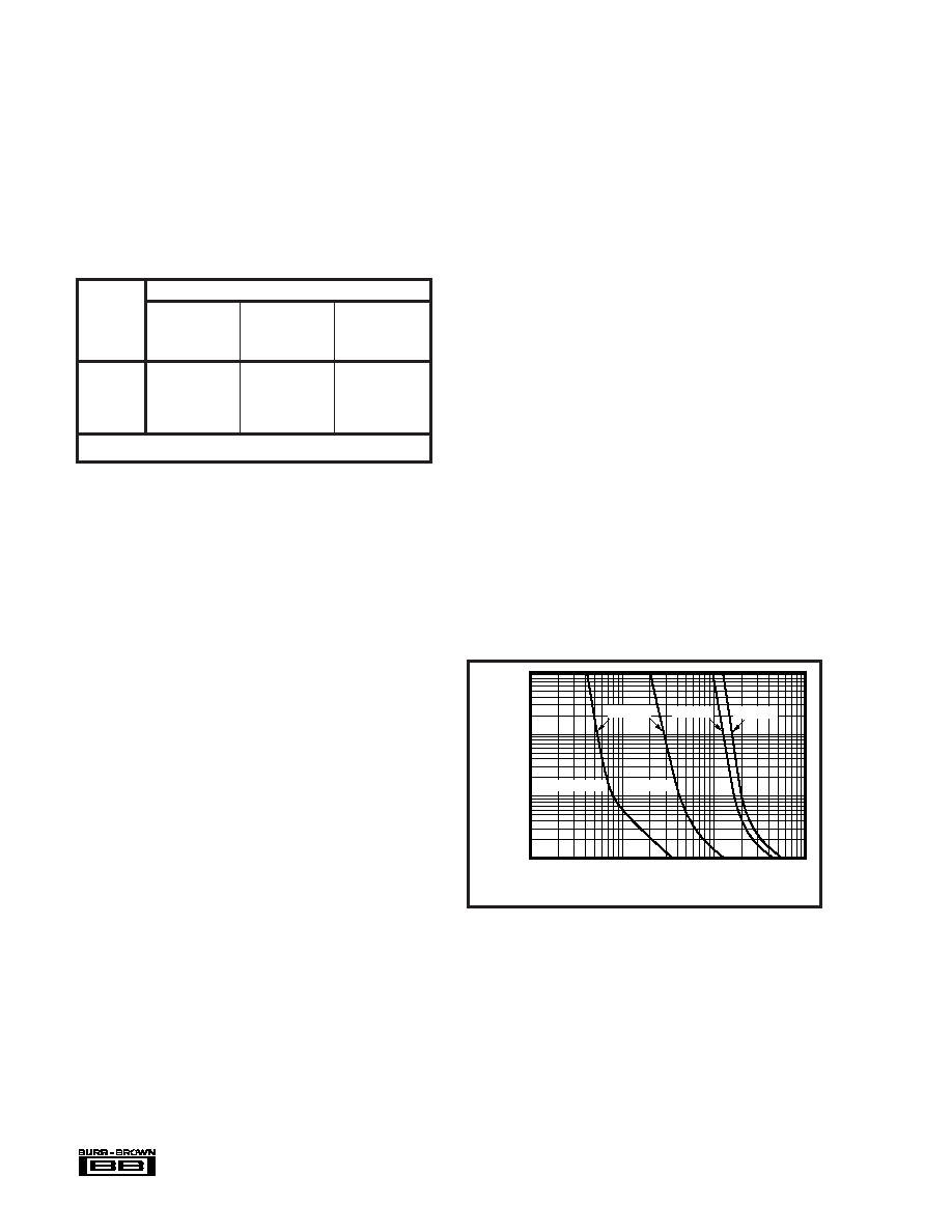
SETTLING TIME
Settling time of the D/A is the total time required for the
analog output to settle within an error band around its final
value after a change in digital input. Refer to Figure 1 for
typical values for this family of products.
Voltage Output
Settling times are specified to
±0.003% of FSR (±1/2LSB
for 14 bits) for two input conditions: a full-scale range
change of 20V (DAC703) or 10V (DAC701) and a 1LSB
change at the “major carry,” the point at which the worst-
case settling time occurs. (This is the worst-case point since
all of the input bits change when going from one code to the
next).
Current Output
Settling times are specified to
±0.003% of FSR for a full-
scale range change for two output load conditions: one for
10
to 100 and one for 1000. It is specified this way
because the output RC time constant becomes the dominant
factor in determining settling time for large resistive loads.
ANALOG OUTPUT
DAC701
DAC702/703
DIGITAL
Complementary
INPUT
Straight Binary
Offset Binary
Two’s Complement
CODES
(CSB)
(COB)
(CTC)*
0000H
+ Full Scale
–1LSB
7FFFH
+1/2 Full Scale
Bipolar Zero
– Full Scale
8000H
+1/2 Full Scale
–1LSB
+ Full Scale
–1LSB
FFFFH
Zero
– Full Scale
Bipolar Zero
* Invert the MSB of the COB code with an external inverter to obtain CTC
code.
TABLE I. Digital Input Codes.
ACCURACY
Linearity
This specification describes one of the most important mea-
sures of performance of a D/A converter. Linearity error is
the deviation of the analog output from a straight line drawn
through the end points (all bits ON point and all bits OFF
point).
Differential Linearity Error
Differential linearity error (DLE) of a D/A converter is the
deviation from an ideal 1LSB change in the output from one
adjacent output state to the next. A differential linearity error
specification of
±1/2LSB means that the output step sizes
can be between 1/2LSB and 3/2LSB when the input changes
from one adjacent input state to the next. A negative DLE
specification of no more than –1LSB (–0.006% for 14-bit
resolution) insures monotonicity.
Monotonicity
Monotonicity assures that the analog output will increase or
remain the same for increasing input digital codes. The
DAC701/702/703 are specified to be monotonic to 14 bits
over the entire specification temperature range.
DRIFT
Gain Drift
Gain drift is a measure of the change in the full-scale range
output over temperature expressed in parts per million per
degree centigrade (ppm/
°C). Gain drift is established by: (1)
testing the end point differences for each D/A at t
MIN, +25°C
and tMAX; (2) calculating the gain error with respect to the
+25
°C value; and (3) dividing by the temperature change.
FIGURE 1. Final-Value Error Band vs Full-Scale Range
Settling Time.
COMPLIANCE VOLTAGE
Compliance voltage applies only to current output models. It
is the maximum voltage swing allowed on the output current
pin while still being able to maintain specified accuracy.
Final-Value
Error
Band,
Percent
of
Full-Scale
Range
(±%
of
FSR)
Settling Time (s)
0.01
0.1
1
10
1
0.1
0.01
0.001
DAC702
DAC701
DAC703
R
L = 100
R
L = 1k
相关PDF资料 |
PDF描述 |
|---|---|
| DAC7545KUG4 | PARALLEL, WORD INPUT LOADING, 2 us SETTLING TIME, 12-BIT DAC, PDSO20 |
| DAC7545JP | PARALLEL, WORD INPUT LOADING, 2 us SETTLING TIME, 12-BIT DAC, PDIP20 |
| DAC7545KP | PARALLEL, WORD INPUT LOADING, 2 us SETTLING TIME, 12-BIT DAC, PDIP20 |
| DAC7554IDGSR | SERIAL INPUT LOADING, 5 us SETTLING TIME, 12-BIT DAC, PDSO10 |
| DAC7554IDGS | SERIAL INPUT LOADING, 5 us SETTLING TIME, 12-BIT DAC, PDSO10 |
相关代理商/技术参数 |
参数描述 |
|---|---|
| DAC702SH | 制造商:BB 制造商全称:BB 功能描述:Monolithic 16-Bit DIGITAL-TO-ANALOG CONVERTERS |
| DAC703 | 制造商:BB 制造商全称:BB 功能描述:Monolithic 16-Bit DIGITAL-TO-ANALOG CONVERTERS |
| DAC703B | 制造商:BB 制造商全称:BB 功能描述:Monolithic 16-Bit DIGITAL-TO-ANALOG CONVERTERS |
| DAC703BH | 制造商:BB 制造商全称:BB 功能描述:Monolithic 16-Bit DIGITAL-TO-ANALOG CONVERTERS |
| DAC703BH-BI | 制造商:BB 制造商全称:BB 功能描述:Monolithic 16-Bit DIGITAL-TO-ANALOG CONVERTERS |
发布紧急采购,3分钟左右您将得到回复。