- 您现在的位置:买卖IC网 > PDF目录170654 > DAC7554IDGSR (TEXAS INSTRUMENTS INC) SERIAL INPUT LOADING, 5 us SETTLING TIME, 12-BIT DAC, PDSO10 PDF资料下载
参数资料
| 型号: | DAC7554IDGSR |
| 厂商: | TEXAS INSTRUMENTS INC |
| 元件分类: | DAC |
| 英文描述: | SERIAL INPUT LOADING, 5 us SETTLING TIME, 12-BIT DAC, PDSO10 |
| 封装: | GREEN, PLASTIC, MSOP-10 |
| 文件页数: | 8/23页 |
| 文件大小: | 1224K |
| 代理商: | DAC7554IDGSR |
www.ti.com
THEORY OF OPERATION
DAC External Reference Input
D/A SECTION
Power-On Reset
_
+
Resistor String
Ref +
Ref
DAC Register
VOUT
REFIN
GND
Power Down
REFIN
To Output
Amplifier
R
GND
SERIAL INTERFACE
RESISTOR STRING
16-Bit Word and Input Shift Register
OUTPUT BUFFER AMPLIFIERS
DAC7554
SLAS399A – OCTOBER 2004 – REVISED NOVEMBER 2004
There is a single reference input pin for the four
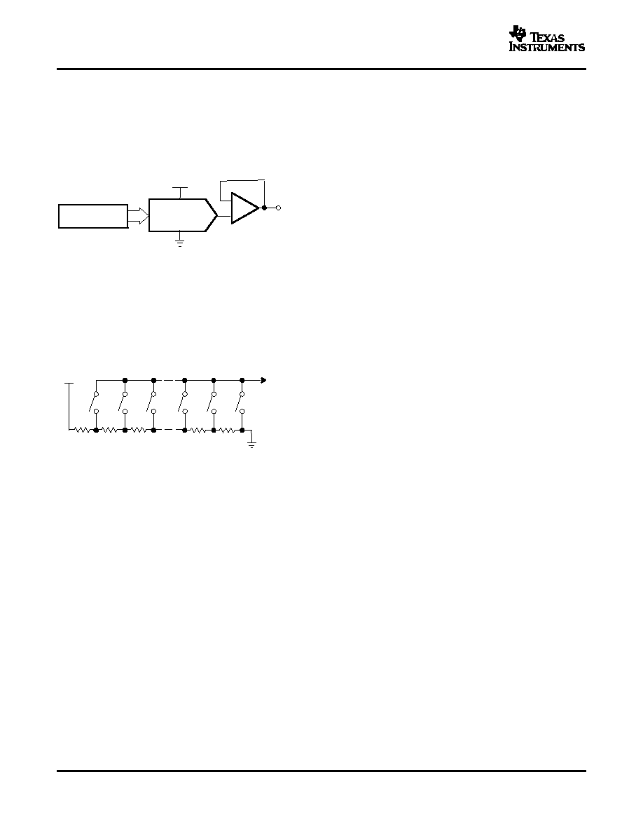
The architecture of the DAC7554 consists of a string
DACs. The reference input is unbuffered. The user
DAC followed by an output buffer amplifier. Figure 33
can have a reference voltage as low as 0.25 V and
shows a generalized block diagram of the DAC
as high as VDD because there is no restriction due to
architecture.
headroom and footroom of any reference amplifier.
It is recommended to use a buffered reference in the
external circuit (e.g., REF3140). The input impedance
is typically 25 k
.
On power up, all internal registers are cleared and all
Figure 33. Typical DAC Architecture
channels are updated with zero-scale voltages. Until
valid data is written, all DAC outputs remain in this
state. This is particularly useful in applications where
The input coding to the DAC7554 is unsigned binary,
it is important to know the state of the DAC outputs
which gives the ideal output voltage as:
while the device is powering up. In order not to turn
VOUT = REFIN × D/4096
on ESD protection devices, VDD should be applied
Where D = decimal equivalent of the binary code that
before any other pin is brought high.
is loaded to the DAC register which can range from 0
to 4095.
The DAC7554 has a flexible power-down capability
as described in Table 2. Individual channels could be
powered down separately or all channels could be
powered down simultaneously. During a power-down
condition, the user has flexibility to select the output
impedance of each channel. During power-down
operation, each channel can have either 1-k
,
100-k
, or Hi-Z output impedance to ground.
Figure 34. Typical Resistor String
The DAC7554 is controlled over a versatile 3-wire
serial interface, which operates at clock rates up to
The resistor string section is shown in Figure 34. It is
50 MHz and is compatible with SPI, QSPI, Microwire,
simply a string of resistors, each of value R. The
and DSP interface standards.
digital code loaded to the DAC register determines at
which node on the string the voltage is tapped off to
be fed into the output amplifier. The voltage is tapped
off by closing one of the switches connecting the
The input shift register is 16 bits wide. DAC data is
string to the amplifier. Because it is a string of
loaded into the device as a 16-bit word under the
resistors, it is specified monotonic. The DAC7554
control of a serial clock input, SCLK, as shown in the
architecture uses four separate resistor strings to
Figure 1 timing diagram. The 16-bit word, illustrated
minimize channel-to-channel crosstalk.
in Table 1, consists of four control bits followed by 12
bits of DAC data. The data format is straight binary
with all zeroes corresponding to 0-V output and all
ones corresponding to full-scale output (VREF – 1
The output buffer amplifier is capable of generating
LSB). Data is loaded MSB first (Bit 15) where the first
rail-to-rail voltages on its output, which gives an
two bits (LD1 and LD0) determine if the input register,
output range of 0 V to VDD. It is capable of driving a
DAC register, or both are updated with shift register
load of 2 k
in parallel with up to 1000 pF to GND.
input data. Bit 13 and bit 12 (Sel1 and Sel0)
The source and sink capabilities of the output ampli-
determine whether the data is for DAC A, DAC B,
fier can be seen in the typical curves. The slew rate is
DAC C, DAC D, or all DACs. All channels are
1 V/s with a half-scale settling time of 3 s with the
updated when bits 15 and 14 (LD1 and LD0) are
output unloaded.
high.
16
相关PDF资料 |
PDF描述 |
|---|---|
| DAC7554IDGS | SERIAL INPUT LOADING, 5 us SETTLING TIME, 12-BIT DAC, PDSO10 |
| DAC7612U | SERIAL INPUT LOADING, 7 us SETTLING TIME, 12-BIT DAC, PDSO8 |
| DAC7612UBG4 | SERIAL INPUT LOADING, 7 us SETTLING TIME, 12-BIT DAC, PDSO8 |
| DAC7625U/1KG4 | PARALLEL, WORD INPUT LOADING, 5 us SETTLING TIME, 12-BIT DAC, PDSO28 |
| DAC7643VFBTG4 | PARALLEL, WORD INPUT LOADING, 8 us SETTLING TIME, 16-BIT DAC, PQFP32 |
相关代理商/技术参数 |
参数描述 |
|---|---|
| DAC7554IDGSRG4 | 功能描述:数模转换器- DAC Low-Power Low-Glitch 12-Bit DAC RoHS:否 制造商:Texas Instruments 转换器数量:1 DAC 输出端数量:1 转换速率:2 MSPs 分辨率:16 bit 接口类型:QSPI, SPI, Serial (3-Wire, Microwire) 稳定时间:1 us 最大工作温度:+ 85 C 安装风格:SMD/SMT 封装 / 箱体:SOIC-14 封装:Tube |
| DAC7558 | 制造商:TI 制造商全称:Texas Instruments 功能描述:12-BIT, OCTAL, ULTRALOW GLITCH, VOLTAGE OUTPUT DIGITAL-TO-ANALOG CONVERTER |
| DAC7558EVM | 功能描述:数据转换 IC 开发工具 DAC7558 Eval Mod RoHS:否 制造商:Texas Instruments 产品:Demonstration Kits 类型:ADC 工具用于评估:ADS130E08 接口类型:SPI 工作电源电压:- 6 V to + 6 V |
| DAC7558IRHBR | 功能描述:数模转换器- DAC 12-Bit Octal UltrLo Glitch Vltg Output RoHS:否 制造商:Texas Instruments 转换器数量:1 DAC 输出端数量:1 转换速率:2 MSPs 分辨率:16 bit 接口类型:QSPI, SPI, Serial (3-Wire, Microwire) 稳定时间:1 us 最大工作温度:+ 85 C 安装风格:SMD/SMT 封装 / 箱体:SOIC-14 封装:Tube |
| DAC7558IRHBRG4 | 功能描述:数模转换器- DAC 12-Bit Octal UltrLo Glitch Vltg Output RoHS:否 制造商:Texas Instruments 转换器数量:1 DAC 输出端数量:1 转换速率:2 MSPs 分辨率:16 bit 接口类型:QSPI, SPI, Serial (3-Wire, Microwire) 稳定时间:1 us 最大工作温度:+ 85 C 安装风格:SMD/SMT 封装 / 箱体:SOIC-14 封装:Tube |
发布紧急采购,3分钟左右您将得到回复。