- 您现在的位置:买卖IC网 > PDF目录170654 > DAC8501E/250G4 (TEXAS INSTRUMENTS INC) SERIAL INPUT LOADING, 12 us SETTLING TIME, 16-BIT DAC, PDSO8 PDF资料下载
参数资料
| 型号: | DAC8501E/250G4 |
| 厂商: | TEXAS INSTRUMENTS INC |
| 元件分类: | DAC |
| 英文描述: | SERIAL INPUT LOADING, 12 us SETTLING TIME, 16-BIT DAC, PDSO8 |
| 封装: | GREEN, PLASTIC, MSOP-8 |
| 文件页数: | 12/20页 |
| 文件大小: | 531K |
| 代理商: | DAC8501E/250G4 |
DAC8501
2
SBAS212A
www.ti.com
VDD to GND ........................................................................... –0.3V to +6V
Digital Input Voltage to GND ................................. –0.3V to +VDD + 0.3V
VOUT to GND .......................................................... –0.3V to +VDD + 0.3V
VREF to GND ........................................................... –0.3V to +VDD + 0.3V
VFB to GND ............................................................. –0.3V to +VDD + 0.3V
Operating Temperature Range ...................................... –40
°C to +105°C
Storage Temperature Range ......................................... –65
°C to +150°C
Junction Temperature Range (TJ max) ........................................ +150°C
Power Dissipation ........................................................ (TJ max — TA)/θJA
θ
JA Thermal Impedance ......................................................... 206°C/W
θ
JC Thermal Impedance ........................................................... 44°C/W
Lead Temperature, Soldering:
Vapor Phase (60s) ............................................................... +215
°C
Infrared (15s) ........................................................................ +220
°C
NOTE: (1) Stresses above those listed under
Absolute Maximum Ratings may
cause permanent damage to the device. Exposure to absolute maximum
conditions for extended periods may affect device reliability.
ABSOLUTE MAXIMUM RATINGS(1)
PACKAGE/ORDERING INFORMATION
RELATIVE
DIFFERENTIAL
SPECIFICATION
ACCURACY
NONLINEARITY
PACKAGE
TEMPERATURE
PACKAGE
ORDERING
TRANSPORT
PRODUCT
(LSB)
PACKAGE-LEAD DESIGNATOR(1)
RANGE
MARKING
NUMBER
MEDIA, QUANTITY
DAC8501E
±64
±1
MSOP-8
DGK
–40
°C to +105°C
D01
DAC8501E/250
Tape and Reel, 250
""
"
DAC8501E/2K5
Tape and Reel, 2500
NOTE: (1) For the most current specifications and package information, refer to our web site at www.ti.com.
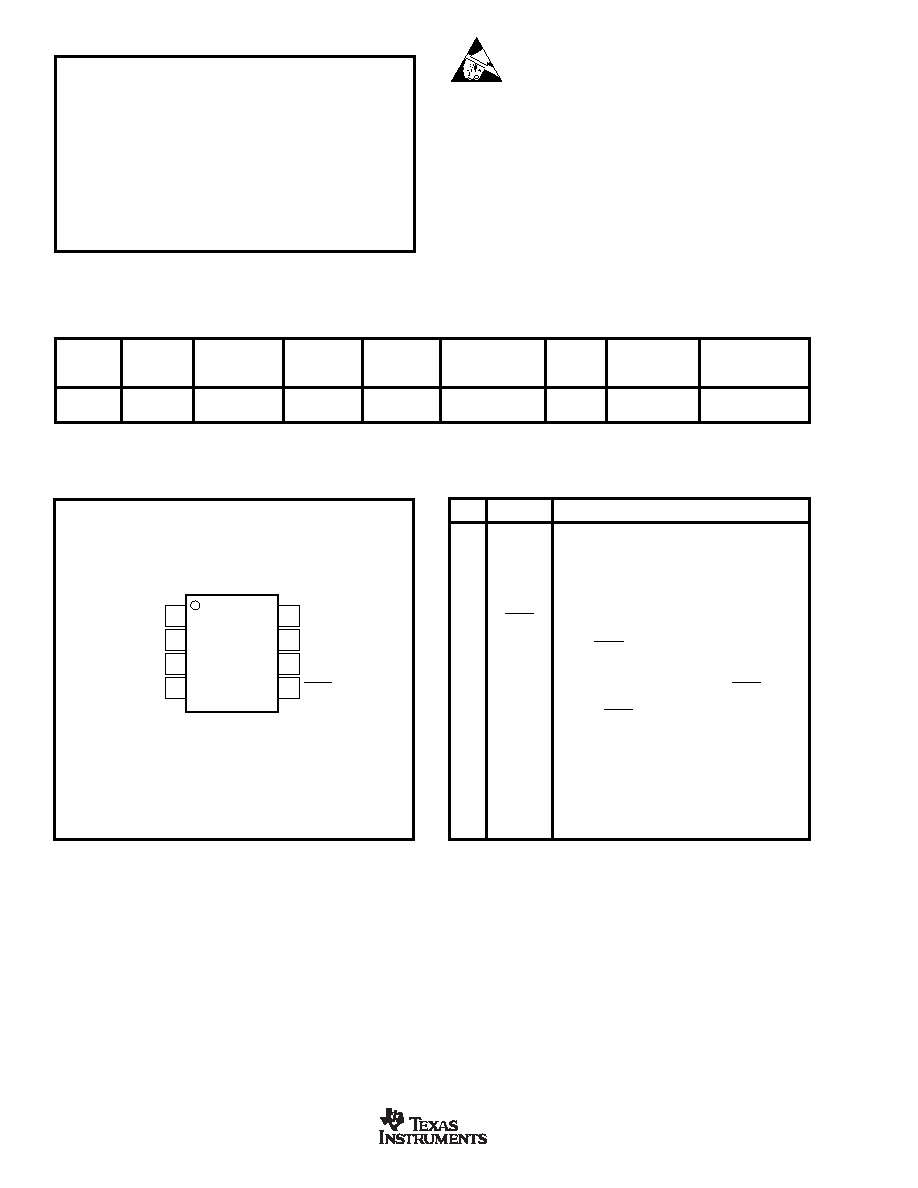
PIN
NAME
DESCRIPTION
1VDD
Power-Supply Input, +2.7V to +5.5V
2VREF
Reference Voltage Input
3VFB
Feedback connection for the output amplifier.
4VOUT
Analog output voltage from DAC. The output ampli-
fier has rail-to-rail operation.
5
SYNC
Level-triggered control input (active LOW). This is
the frame synchronization signal for the input data.
When SYNC goes LOW, it enables the input shift
register and data is transferred in on the falling
edges of the following clocks. The DAC is updated
following the 24th clock cycle unless SYNC is taken
HIGH before this edge, in which case the rising
edge of SYNC acts as an interrupt and the write
sequence is ignored by the DAC8501.
6
SCLK
Serial Clock Input. Data can be transferred at rates
up to 30MHz.
7DIN
Serial Data Input. Data is clocked into the 24-bit
input shift register on the falling edge of the serial
clock input.
8
GND
Ground reference point for all circuitry on the part.
PIN DESCRIPTION
PIN CONFIGURATIONS
Top View
MSOP
V
DD
V
REF
V
FB
V
OUT
GND
D
IN
SCLK
SYNC
1
2
3
4
8
7
6
5
DAC8501
ELECTROSTATIC
DISCHARGE SENSITIVITY
This integrated circuit can be damaged by ESD. Texas Instru-
ments recommends that all integrated circuits be handled with
appropriate precautions. Failure to observe proper handling
and installation procedures can cause damage.
ESD damage can range from subtle performance degradation
to complete device failure. Precision integrated circuits may be
more susceptible to damage because very small parametric
changes could cause the device not to meet its published
specifications.
相关PDF资料 |
PDF描述 |
|---|---|
| DAC8551IADGKR | SERIAL INPUT LOADING, 12 us SETTLING TIME, 16-BIT DAC, PDSO8 |
| DAC8551IADGKTG4 | SERIAL INPUT LOADING, 12 us SETTLING TIME, 16-BIT DAC, PDSO8 |
| DAC8551IADGKT | SERIAL INPUT LOADING, 12 us SETTLING TIME, 16-BIT DAC, PDSO8 |
| DAC8551IADGKRG4 | SERIAL INPUT LOADING, 12 us SETTLING TIME, 16-BIT DAC, PDSO8 |
| DAC8554IPWR | SERIAL INPUT LOADING, 12 us SETTLING TIME, 16-BIT DAC, PDSO16 |
相关代理商/技术参数 |
参数描述 |
|---|---|
| DAC8501E2K5 | 制造商:BB 制造商全称:BB 功能描述:Low-Power, Rail-to-Rail Output, 16-Bit Serial Input DIGITAL-TO-ANALOG CONVERTER |
| DAC8512 | 制造商:Analog Devices 功能描述:DAC8512 |
| DAC8512002S | 制造商:Analog Devices 功能描述: |
| DAC8512-002S | 制造商:Analog Devices 功能描述: |
| DAC8512EP | 功能描述:IC DAC 12BIT SRL LP 5V 8-DIP RoHS:否 类别:集成电路 (IC) >> 数据采集 - 数模转换器 系列:- 产品培训模块:Data Converter Fundamentals DAC Architectures 标准包装:750 系列:- 设置时间:7µs 位数:16 数据接口:并联 转换器数目:1 电压电源:双 ± 功率耗散(最大):100mW 工作温度:0°C ~ 70°C 安装类型:表面贴装 封装/外壳:28-LCC(J 形引线) 供应商设备封装:28-PLCC(11.51x11.51) 包装:带卷 (TR) 输出数目和类型:1 电压,单极;1 电压,双极 采样率(每秒):143k |
发布紧急采购,3分钟左右您将得到回复。