- 您现在的位置:买卖IC网 > PDF目录170654 > DAC8501E/250G4 (TEXAS INSTRUMENTS INC) SERIAL INPUT LOADING, 12 us SETTLING TIME, 16-BIT DAC, PDSO8 PDF资料下载
参数资料
| 型号: | DAC8501E/250G4 |
| 厂商: | TEXAS INSTRUMENTS INC |
| 元件分类: | DAC |
| 英文描述: | SERIAL INPUT LOADING, 12 us SETTLING TIME, 16-BIT DAC, PDSO8 |
| 封装: | GREEN, PLASTIC, MSOP-8 |
| 文件页数: | 4/20页 |
| 文件大小: | 531K |
| 代理商: | DAC8501E/250G4 |
DAC8501
12
SBAS212A
www.ti.com
SERIAL INTERFACE
The DAC8501 has a 3-wire serial interface (SYNC, SCLK, and
DIN), which is compatible with SPI, QSPI, and Microwire interface
standards as well as most DSPs, (see the Serial Write Operation
timing diagram for an example of a typical write sequence).
The write sequence begins by bringing the SYNC line LOW, data
from the DIN line is clocked into the 24-bit shift register on the
falling edge of SCLK. The serial clock frequency can be as high
as 30MHz, making the DAC8501 compatible with high-speed
DSPs. On the 24th falling edge of the serial clock, the last data
bit is clocked in and the programmed function is executed (i.e., a
change in DAC register contents and/or a change in the mode of
operation).
At this point, the SYNC line can be kept LOW or brought HIGH.
In either case, it must be brought HIGH for a minimum of 33ns
before the next write sequence so that a falling edge of SYNC
can initiate the next write sequence. As the SYNC buffer draws
more current when the SYNC signal is HIGH than it does when
it is LOW, SYNC must be idled LOW between write sequences
for lowest power operation of the part; as mentioned above, it
must be brought HIGH again just before the next write sequence.
INPUT SHIFT REGISTER
The input shift register is 24 bits wide, as shown in
Figure 3. The first six bits are
don’t cares. The next two bits (PD1
and PD0) are control bits that control which mode of operation the
part is in (normal mode or any one of three power-down modes):
there is a more complete description of the various modes in the
Power-Down Modes section. The next 16 bits are the data bits
which are transferred to the DAC register on the 24th falling edge
of SCLK.
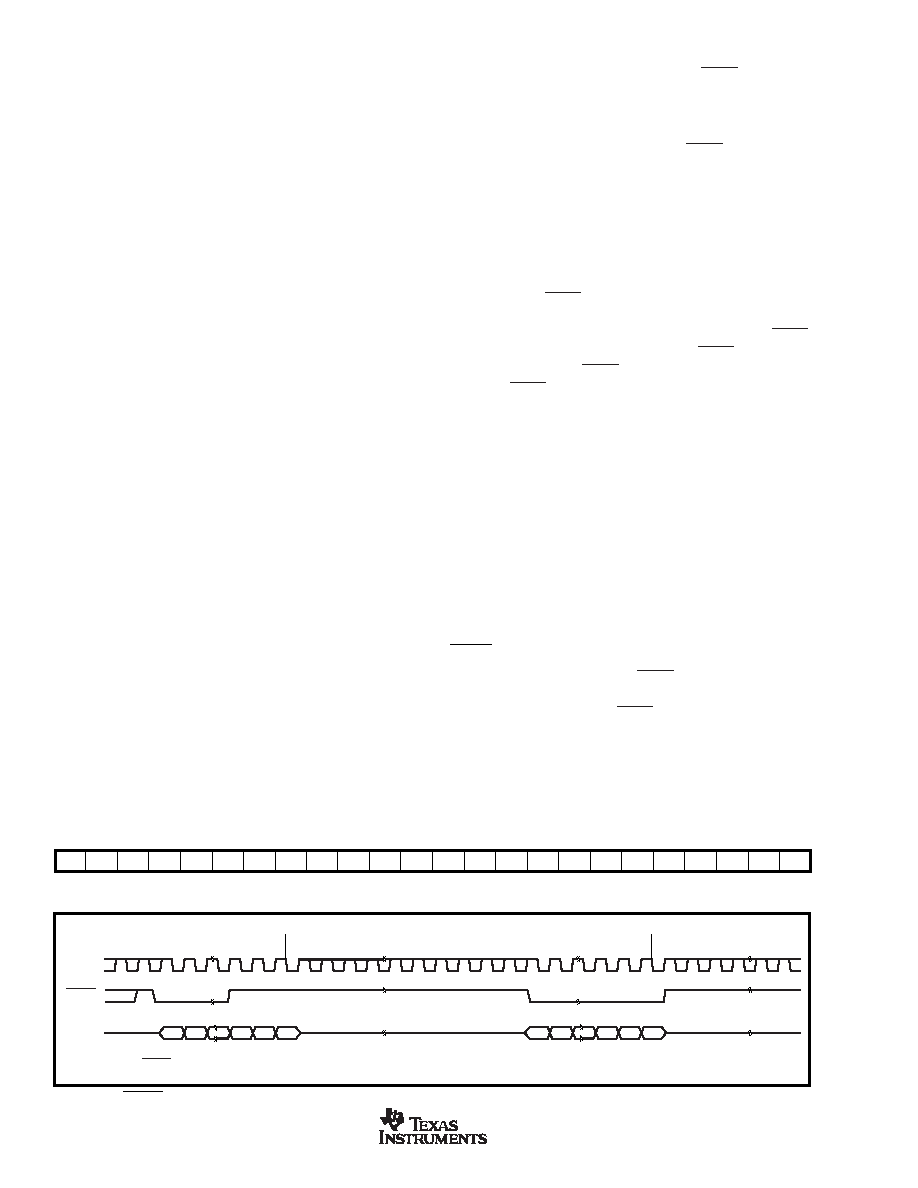
SYNC INTERRUPT
In a normal write sequence, the SYNC line is kept LOW for at
least 24 falling edges of SCLK and the DAC is updated on the
24th falling edge. However, if SYNC is brought HIGH before the
24th falling edge, this acts as an interrupt to the write sequence.
When this happens, the shift register is reset and the write
sequence is seen as invalid. Neither an update of the DAC
register contents or a change in the operating mode occurs, as
shown in Figure 4.
XXXX
X
PD1
PD0
D15
D14
D13
D12
D11
D10
D9
D8
D7
D6
D5
D4
D3
D2
D1
D0
FIGURE 3. Data Input Register.
FIGURE 4. SYNC Interrupt Facility.
DB23
DB0
OUTPUT AMPLIFIER
The output buffer amplifier is capable of generating rail-to-rail
voltages on its output which gives an output range of
0V to VDD; it is capable of driving a load of 2k in parallel with
1000pF to GND. The source and sink capabilities of the
output amplifier can be seen in the typical characteristics.
The slew rate is 1V/
s with a full-scale settling time of 8s
with the output unloaded.
The inverting input of the output amplifier is brought out to the
VFB pin which allows for better accuracy in critical applica-
tions by tying the VFB point and the amplifier output together
directly at the load. Other signal conditioning circuitry may
also be connected between these points for specific applica-
tions.
MULTIPLYING MODE OPTIMIZATIONS
The DAC8501 is a version of the DAC8531 optimized for
multiplying mode at a typical bandwidth of up to 350kHz,
which gives better phase and gain performance.
Two aspects of the DAC8501 operation are affected by the
optimizations. The resistor string in the DAC8531 is discon-
nected from the reference input when power-down mode is
entered, but in the DAC8501, the resistor string continues to
draw current from the reference input during power-down
mode.
The DAC8501 has slightly different offset characteristics
from the DAC8531: the DAC8501 may output 0V for the first
few hundred codes, whereas the DAC8531 typically has far
fewer such dead codes near 0. Offset and gain errors are
measured from code 0200H for both devices, so specifica-
tions are not affected. In all other respects, the DAC8531 and
DAC8501 operate identically.
Multiplying-mode bandwidth is measured at both small-signal
and full-power levels. Bandwidth at full-power amplitude,
which is typically 64kHz, is limited by the 1V/
s slew rate of
the output amplifier. Small-amplitude signals that do not
cause the amplifier to slew are bandlimited by the output
amplifier to approximately 350kHz. If the design approaches
either of these limits, the DAC8501 must be tested in the
application to ensure that it meets the needed requirements.
CLK
SYNC
D
IN
Invalid Write Sequence:
SYNC HIGH before 24th Falling Edge
Valid Write Sequence: Output Updates
on the 24th Falling Edge
DB23
DB0
DB23
DB0
24th Falling Edge
相关PDF资料 |
PDF描述 |
|---|---|
| DAC8551IADGKR | SERIAL INPUT LOADING, 12 us SETTLING TIME, 16-BIT DAC, PDSO8 |
| DAC8551IADGKTG4 | SERIAL INPUT LOADING, 12 us SETTLING TIME, 16-BIT DAC, PDSO8 |
| DAC8551IADGKT | SERIAL INPUT LOADING, 12 us SETTLING TIME, 16-BIT DAC, PDSO8 |
| DAC8551IADGKRG4 | SERIAL INPUT LOADING, 12 us SETTLING TIME, 16-BIT DAC, PDSO8 |
| DAC8554IPWR | SERIAL INPUT LOADING, 12 us SETTLING TIME, 16-BIT DAC, PDSO16 |
相关代理商/技术参数 |
参数描述 |
|---|---|
| DAC8501E2K5 | 制造商:BB 制造商全称:BB 功能描述:Low-Power, Rail-to-Rail Output, 16-Bit Serial Input DIGITAL-TO-ANALOG CONVERTER |
| DAC8512 | 制造商:Analog Devices 功能描述:DAC8512 |
| DAC8512002S | 制造商:Analog Devices 功能描述: |
| DAC8512-002S | 制造商:Analog Devices 功能描述: |
| DAC8512EP | 功能描述:IC DAC 12BIT SRL LP 5V 8-DIP RoHS:否 类别:集成电路 (IC) >> 数据采集 - 数模转换器 系列:- 产品培训模块:Data Converter Fundamentals DAC Architectures 标准包装:750 系列:- 设置时间:7µs 位数:16 数据接口:并联 转换器数目:1 电压电源:双 ± 功率耗散(最大):100mW 工作温度:0°C ~ 70°C 安装类型:表面贴装 封装/外壳:28-LCC(J 形引线) 供应商设备封装:28-PLCC(11.51x11.51) 包装:带卷 (TR) 输出数目和类型:1 电压,单极;1 电压,双极 采样率(每秒):143k |
发布紧急采购,3分钟左右您将得到回复。