- 您现在的位置:买卖IC网 > PDF目录170654 > DAC8501E/250G4 (TEXAS INSTRUMENTS INC) SERIAL INPUT LOADING, 12 us SETTLING TIME, 16-BIT DAC, PDSO8 PDF资料下载
参数资料
| 型号: | DAC8501E/250G4 |
| 厂商: | TEXAS INSTRUMENTS INC |
| 元件分类: | DAC |
| 英文描述: | SERIAL INPUT LOADING, 12 us SETTLING TIME, 16-BIT DAC, PDSO8 |
| 封装: | GREEN, PLASTIC, MSOP-8 |
| 文件页数: | 5/20页 |
| 文件大小: | 531K |
| 代理商: | DAC8501E/250G4 |
DAC8501
13
SBAS212A
www.ti.com
POWER-ON RESET
The DAC8501 contains a power-on reset circuit that controls
the output voltage during power-up. On power-up, the DAC
register is filled with zeros and the output voltage is 0V; it
remains there until a valid write sequence is made to the
DAC. This is useful in applications where it is important to
know the state of the output of the DAC when it is in the
process of powering up.
POWER-DOWN MODES
The DAC8501 supports four separate modes of operation
which are programmable by setting two bits (PD1 and PD0)
in the control register. Table I shows how the state of the bits
corresponds to the mode of operation of the device.
MICROPROCESSOR
INTERFACING
DAC8501 TO 8051 INTERFACE
Figure 6 shows a serial interface between the DAC8501 and
a typical 8051-type microcontroller. The setup for the inter-
face is as follows: TXD of the 8051 drives SCLK of the
DAC8501, whereas RXD drives the serial data line of the
part. The SYNC signal is derived from a bit-programmable
pin on the port, in this case, port line P3.3 is used. When data
is to be transmitted to the DAC8501, P3.3 is taken LOW. The
8051 transmits data only in 8-bit bytes; thus only eight falling
clock edges occur in the transmit cycle. To load data to the
DAC, P3.3 is left LOW after the first eight bits are transmitted,
and a second write cycle is initiated to transmit the second
byte of data. P3.3 is taken HIGH following the completion of
the third write cycle. The 8051 outputs the serial data in a
format which has the LSB first. The DAC8501 requires its
data with the MSB as the first bit received, therefore the 8051
transmit routine must take this into account, and mirror the
data as needed.
PD1 (DB17)
PD0 (DB16)
OPERATING MODE
0
Normal Operation
——
Power-Down Modes
0
1
Output 1k
to GND
1
0
Output 100k
to GND
1
High-Z
TABLE I. Modes of Operation for the DAC8501.
DAC8501 TO Microwire INTERFACE
Figure 7 shows an interface between the DAC8501 and any
Microwire compatible device. Serial data is shifted out on the
falling edge of the serial clock and is clocked into the
DAC8501 on the rising edge of the SK signal.
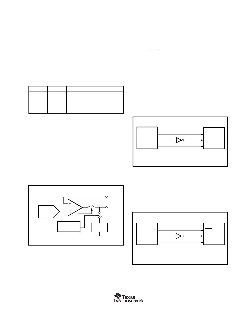
FIGURE 5. Output Stage During Power-Down.
All linear circuitry is shut down when the power-down mode
is activated, however, the contents of the DAC register are
unaffected when in power-down. The time to exit power-
down is typically 2.5
s for V
DD = 5V, and 5s for VDD = 3V,
(see the Typical Characteristics for more information).
When both bits are set to 0, the part works normally with its
typical current consumption of 250
A at 5V; however, for the
three power-down modes, the supply current falls to 200nA
at 5V (50nA at 3V). Not only does the supply current fall, but
the output stage is also internally switched from the output of
the amplifier to a resistor network of known values, this has
the advantage that the output impedance of the part is known
while the part is in power-down mode. There are three
different options: the output is connected internally to GND
through a 1k
resistor; a 100k resistor; or it is left open-
circuited (High-Z), Figure 5 shows the output stage.
FIGURE 6. DAC8501 to 80C51/80L51 Interface.
FIGURE 7. DAC8501 to Microwire Interface.
Resistor
String DAC
Amplifier
Power-Down
Circuitry
Resistor
Network
V
OUT
V
FB
80C51/80L51(1)
P3.3
TXD
RXD
DAC8501(1)
SYNC
SCLK
D
IN
NOTE: (1) Additional pins omitted for clarity.
SYNC
SCLK
D
IN
MicrowireTM
CS
SK
SO
DAC8501(1)
NOTE: (1) Additional pins omitted for clarity.
相关PDF资料 |
PDF描述 |
|---|---|
| DAC8551IADGKR | SERIAL INPUT LOADING, 12 us SETTLING TIME, 16-BIT DAC, PDSO8 |
| DAC8551IADGKTG4 | SERIAL INPUT LOADING, 12 us SETTLING TIME, 16-BIT DAC, PDSO8 |
| DAC8551IADGKT | SERIAL INPUT LOADING, 12 us SETTLING TIME, 16-BIT DAC, PDSO8 |
| DAC8551IADGKRG4 | SERIAL INPUT LOADING, 12 us SETTLING TIME, 16-BIT DAC, PDSO8 |
| DAC8554IPWR | SERIAL INPUT LOADING, 12 us SETTLING TIME, 16-BIT DAC, PDSO16 |
相关代理商/技术参数 |
参数描述 |
|---|---|
| DAC8501E2K5 | 制造商:BB 制造商全称:BB 功能描述:Low-Power, Rail-to-Rail Output, 16-Bit Serial Input DIGITAL-TO-ANALOG CONVERTER |
| DAC8512 | 制造商:Analog Devices 功能描述:DAC8512 |
| DAC8512002S | 制造商:Analog Devices 功能描述: |
| DAC8512-002S | 制造商:Analog Devices 功能描述: |
| DAC8512EP | 功能描述:IC DAC 12BIT SRL LP 5V 8-DIP RoHS:否 类别:集成电路 (IC) >> 数据采集 - 数模转换器 系列:- 产品培训模块:Data Converter Fundamentals DAC Architectures 标准包装:750 系列:- 设置时间:7µs 位数:16 数据接口:并联 转换器数目:1 电压电源:双 ± 功率耗散(最大):100mW 工作温度:0°C ~ 70°C 安装类型:表面贴装 封装/外壳:28-LCC(J 形引线) 供应商设备封装:28-PLCC(11.51x11.51) 包装:带卷 (TR) 输出数目和类型:1 电压,单极;1 电压,双极 采样率(每秒):143k |
发布紧急采购,3分钟左右您将得到回复。