- 您现在的位置:买卖IC网 > PDF目录17032 > DC1082A-F (Linear Technology)BOARD SAR ADC LTC2355-14 PDF资料下载
参数资料
| 型号: | DC1082A-F |
| 厂商: | Linear Technology |
| 文件页数: | 14/18页 |
| 文件大小: | 0K |
| 描述: | BOARD SAR ADC LTC2355-14 |
| 软件下载: | QuikEval II System |
| 设计资源: | DC1082A Design File DC1082A Schematic |
| 标准包装: | 1 |
| 系列: | QuikEval-II™ |
| ADC 的数量: | 1 |
| 位数: | 14 |
| 采样率(每秒): | 3M |
| 数据接口: | 串行,SPI? |
| 输入范围: | 0 ~ 2.5 V |
| 已用 IC / 零件: | LTC2355-14 |
| 已供物品: | 板 |
| 相关产品: | LTC2355IMSE-14#TRPBF-ND - IC ADC 14BIT 3.5MSPS 10-MSOP LTC2355CMSE-14#TRPBF-ND - IC ADC 14BIT 3.5MSPS 10-MSOP LTC2355CMSE-12#TRPBF-ND - IC ADC 12BIT 3.5MSPS 10-MSOP LTC2355IMSE-12#TRPBF-ND - IC ADC 12BIT 3.5MSPS 10-MSOP LTC2355IMSE-14#PBF-ND - IC ADC 14BIT 3.5MSPS 10-MSOP LTC2355IMSE-12#PBF-ND - IC ADC 12BIT 3.5MSPS 10-MSOP LTC2355CMSE-14#PBF-ND - IC ADC 14BIT 3.5MSPS 10-MSOP LTC2355CMSE-12#PBF-ND - IC ADC 12BIT 3.5MSPS 10-MSOP |
LTC2355-12/LTC2355-14
2355fa
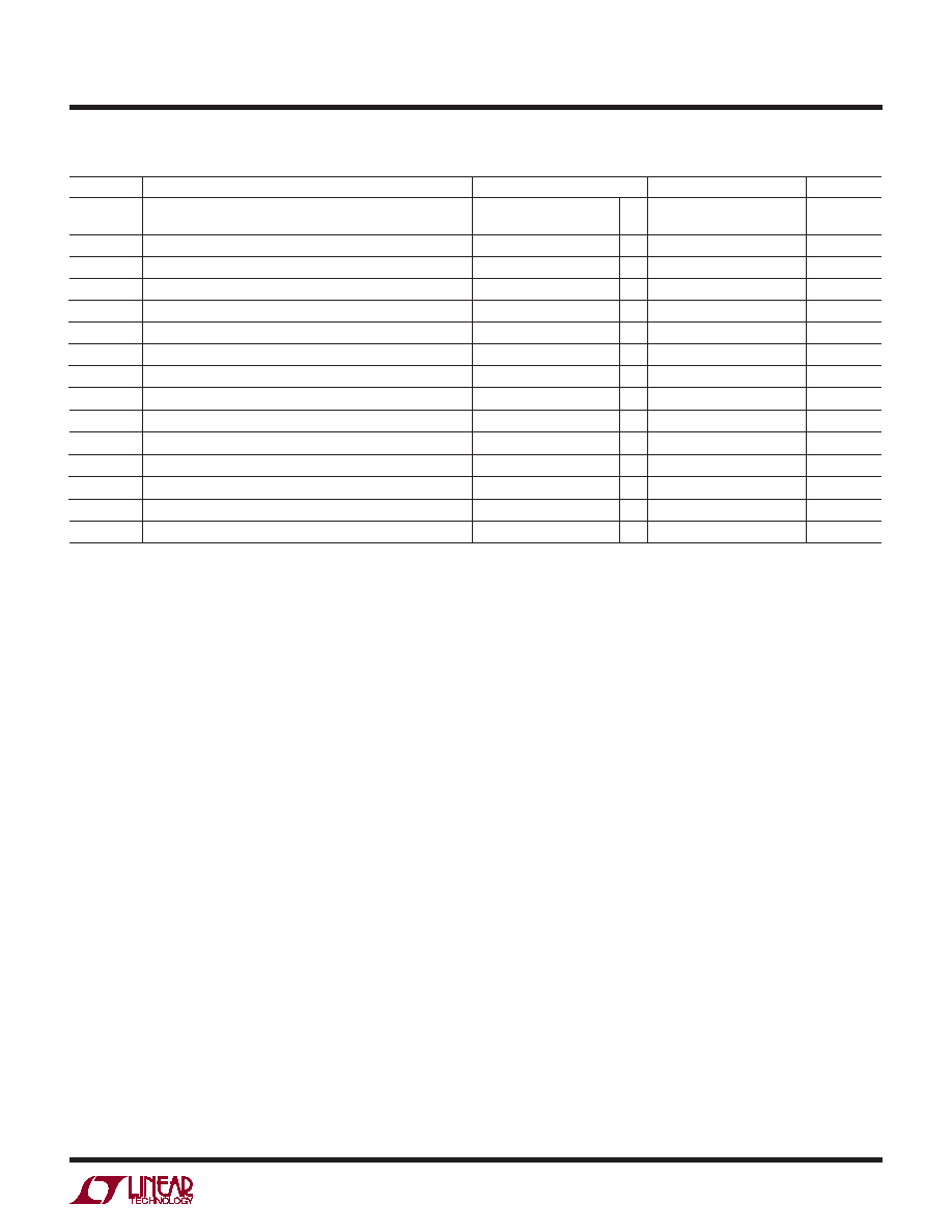
timing characteristics
Note 1: Stresses beyond those listed under Absolute Maximum Ratings
may cause permanent damage to the device. Exposure to any Absolute
Maximum Rating condition for extended periods may affect device
reliability and lifetime.
Note 2: All voltage values are with respect to GND.
Note 3: When these pins are taken below GND or above VDD, they will be
clamped by internal diodes. This product can handle input currents greater
than 100mA below GND or greater than VDD without latchup.
Note 4: Offset and full-gain specifications are measured for a single-ended
AIN+ input with AIN– grounded and using the internal 2.5V reference.
Note 5: Integral linearity is tested with an external 2.55V reference and is
defined as the deviation of a code from the straight line passing through
the actual endpoints of a transfer curve. The deviation is measured from
the center of quantization band.
Note 6: Guaranteed by design, not subject to test.
Note 7: Recommended operating conditions.
Note 8: The analog input range is defined for the voltage difference
between AIN+ and AIN–.
Note 9: The absolute voltage at AIN+ and AIN– must be within this range.
Note 10: If less than 3ns is allowed, the output data will appear one
clock cycle later. It is best for CONV to rise half a clock before SCK, when
running the clock at rated speed.
The l denotes the specifications which apply over the full operating temperature
range, otherwise specifications are at TA = 25°C. VDD = 3.3V.
SYMBOL
PARAMETER
CONDITIONS
MIN
TYP
MAX
UNITS
fSAMPLE(MAX) Maximum Sampling Rate per Channel
(Conversion Rate)
l
3.5
MHz
tTHROUGHPUT Minimum Sampling Period (Conversion + Acquisiton Period)
l
286
ns
tSCK
Clock Period
(Note 16)
l
15.872
10000
ns
tCONV
Conversion Time
(Note 6)
16
18
SCLK cycles
t1
Minimum High or Low SCLK Pulse Width
(Note 6)
2
ns
t2
CONV to SCK Setup Time
(Notes 6, 10)
3
ns
t3
Nearest SCK Edge Before CONV
(Note 6)
0
ns
t4
Minimum High or Low CONV Pulse Width
(Note 6)
4
ns
t5
SCK
↑ to Sample Mode
(Note 6)
4
ns
t6
CONV
↑ to Hold Mode
(Notes 6, 11)
1.2
ns
t7
16th SCK
↑ to CONV↑ Interval (Affects Acquisition Period)
(Notes 6, 7, 13)
45
ns
t8
Delay from SCK to Valid Bits 0 Through 13
(Notes 6, 12)
8
ns
t9
SCK
↑ to Hi-Z at SDO
(Notes 6, 12)
6
ns
t10
Previous SDO Bit Remains Valid After SCK
(Notes 6, 12)
2
ns
t12
VREF Settling Time After Sleep-to-Wake Transition
(Note 14)
2
ms
Note 11: Not the same as aperture delay. Aperture delay is smaller (1ns)
because the 2.2ns delay through the sample-and-hold is subtracted from
the CONV to Hold mode delay.
Note 12: The rising edge of SCK is guaranteed to catch the data coming
out into a storage latch.
Note 13: The time period for acquiring the input signal is started by the
16th rising clock and it is ended by the rising edge of convert.
Note 14: The internal reference settles in 2ms after it wakes up from Sleep
mode with one or more cycles at SCK and a 10F capacitive load.
Note 15: The full power bandwidth is the frequency where the output code
swing drops to 3dB with a 2.5VP-P input sine wave.
Note 16: Maximum clock period guarantees analog performance during
conversion. Output data can be read with an arbitrarily long clock.
Note 17: VDD = 3.3V, fSAMPLE = 3.5Msps.
Note 18: The LTC2355-14 is measured and specified with 14-bit resolution
(1LSB = 152V) and the LTC2355-12 is measured and specified with
12-bit resolution (1LSB = 610V).
Note 19: The sampling capacitor at each input accounts for 4.1pF of the
input capacitance.
相关PDF资料 |
PDF描述 |
|---|---|
| ECE-V0JA102UP | CAP ALUM 1000UF 6.3V 20% SMD |
| STD17W-7 | WIRE & CABLE MARKERS |
| DC1082A-E | BOARD SAR ADC LTC2356-14 |
| FPF2302MPX | IC LOAD SW 2CH LATCH-OFF 8-MLP |
| GCM25DCBD | CONN EDGECARD 50POS R/A .156 SLD |
相关代理商/技术参数 |
参数描述 |
|---|---|
| DC1083A-A | 功能描述:BOARD DEMO LTM4603 RoHS:否 类别:编程器,开发系统 >> 评估板 - DC/DC 与 AC/DC(离线)SMPS 系列:µModule® 标准包装:1 系列:- 主要目的:DC/DC,步降 输出及类型:1,非隔离 功率 - 输出:- 输出电压:3.3V 电流 - 输出:3A 输入电压:4.5 V ~ 28 V 稳压器拓扑结构:降压 频率 - 开关:250kHz 板类型:完全填充 已供物品:板 已用 IC / 零件:L7981 其它名称:497-12113STEVAL-ISA094V1-ND |
| DC1083A-B | 功能描述:BOARD DEMO LTM4603HV RoHS:否 类别:编程器,开发系统 >> 评估板 - DC/DC 与 AC/DC(离线)SMPS 系列:µModule® 标准包装:1 系列:- 主要目的:DC/DC,步降 输出及类型:1,非隔离 功率 - 输出:- 输出电压:3.3V 电流 - 输出:3A 输入电压:4.5 V ~ 28 V 稳压器拓扑结构:降压 频率 - 开关:250kHz 板类型:完全填充 已供物品:板 已用 IC / 零件:L7981 其它名称:497-12113STEVAL-ISA094V1-ND |
| DC1084A-A | 功能描述:BOARD DEMO LTM4602 RoHS:否 类别:编程器,开发系统 >> 评估板 - DC/DC 与 AC/DC(离线)SMPS 系列:µModule® 标准包装:1 系列:- 主要目的:DC/DC,步降 输出及类型:1,非隔离 功率 - 输出:- 输出电压:3.3V 电流 - 输出:3A 输入电压:4.5 V ~ 28 V 稳压器拓扑结构:降压 频率 - 开关:250kHz 板类型:完全填充 已供物品:板 已用 IC / 零件:L7981 其它名称:497-12113STEVAL-ISA094V1-ND |
| DC1084A-B | 功能描述:BOARD DEMO LTM4602HV RoHS:否 类别:编程器,开发系统 >> 评估板 - DC/DC 与 AC/DC(离线)SMPS 系列:µModule® 标准包装:1 系列:- 主要目的:DC/DC,步降 输出及类型:1,非隔离 功率 - 输出:- 输出电压:3.3V 电流 - 输出:3A 输入电压:4.5 V ~ 28 V 稳压器拓扑结构:降压 频率 - 开关:250kHz 板类型:完全填充 已供物品:板 已用 IC / 零件:L7981 其它名称:497-12113STEVAL-ISA094V1-ND |
| DC108R | 制造商:未知厂家 制造商全称:未知厂家 功能描述:Analog IC |
发布紧急采购,3分钟左右您将得到回复。