- 您现在的位置:买卖IC网 > PDF目录16538 > DC1562A-L (Linear Technology)BOARD EVAL LTC6994-2 PDF资料下载
参数资料
| 型号: | DC1562A-L |
| 厂商: | Linear Technology |
| 文件页数: | 26/26页 |
| 文件大小: | 0K |
| 描述: | BOARD EVAL LTC6994-2 |
| 设计资源: | DC1562A Design Files DC1562A Schematic |
| 特色产品: | TimerBlox? |
| 标准包装: | 1 |
| 系列: | TimerBlox® |
| 主要目的: | 定时,延迟线路 |
| 嵌入式: | 否 |
| 已用 IC / 零件: | LTC6994-2 |
| 主要属性: | 100ms 下降沿与上升沿延迟 |
| 次要属性: | 2.25 V ~ 5.5 V 电源 |
| 已供物品: | 板 |
LTC6994-1/LTC6994-2
9
699412fb
pin FuncTions (DCB/S6)
V+ (Pin 1/Pin 5): Supply Voltage (2.25V to 5.5V). This sup-
ply should be kept free from noise and ripple. It should be
bypassed directly to the GND pin with a 0.1F capacitor.
DIV (Pin 2/Pin 4): Programmable Divider and Polarity
Input. The DIV pin voltage (VDIV) is internally converted
into a 4-bit result (DIVCODE). VDIV may be generated by
a resistor divider between V+ and GND. Use 1% resistors
to ensure an accurate result. The DIV pin and resistors
should be shielded from the OUT pin or any other traces
that have fast edges. Limit the capacitance on the DIV pin
to less than 100pF so that VDIV settles quickly. The MSB
of DIVCODE (POL) selects the delay functionality. For the
LTC6994-1, POL = 0 will delay the rising transition and
POL = 1 will delay the falling transition. For the LTC6994-
2, both transitions are delayed so POL = 1 can be used
to invert the output.
SET (Pin 3/Pin 3): Delay Setting Input. The voltage on the
SET pin (VSET) is regulated to 1V above GND. The amount
of current sourced from the SET pin (ISET) programs the
master oscillator frequency. The ISET current range is
1.25A to 20A. The delayed output transition will be not
occur if ISET drops below approximately 500nA. Once ISET
increases above 500nA the delayed edge will transition.
A resistor connected between SET and GND is the most
accurate way to set the delay. For best performance, use
a precision metal or thin film resistor of 0.5% or better
tolerance and 50ppm/°C or better temperature coefficient.
For lower accuracy applications an inexpensive 1% thick
film resistor may be used.
Limit the capacitance on the SET pin to less than 10pF
to minimize jitter and ensure stability. Capacitance less
than 100pF maintains the stability of the feedback circuit
regulating the VSET voltage.
IN(Pin4/Pin1):LogicInput.Dependingontheversionand
POL bit setting, rising or falling edges on IN will propagate
to OUT after a programmable delay. The LTC6994-1 will
delay only the rising or falling edge. The LTC6994-2 will
delay both edges.
GND (Pin 5/Pin 2): Ground. Tie to a low inductance ground
plane for best performance.
OUT (Pin 6/Pin 6): Output. The OUT pin swings from
GND to V+ with an output resistance of approximately
30Ω. When driving an LED or other low impedance load
a series output resistor should be used to limit source/
sink current to 20mA.
699412 PF
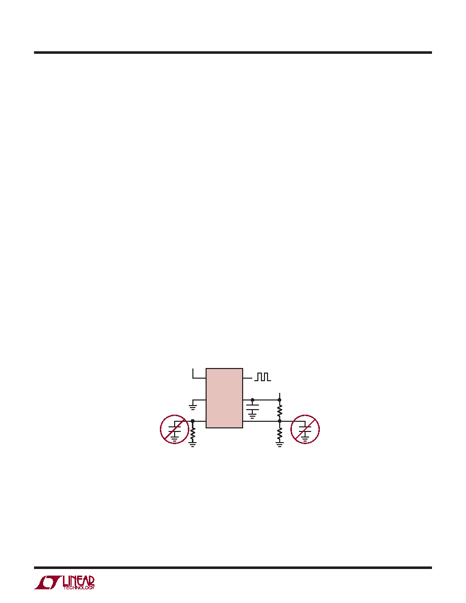
LTC6994
IN
GND
SET
OUT
V+
DIV
C1
0.1F
RSET
R2
R1
V+
相关PDF资料 |
PDF描述 |
|---|---|
| H8PPS-4036G | DIP CABLE - HDP40S/AE40G/HDP40S |
| GEA35DTMN | CONN EDGECARD 70POS R/A .125 SLD |
| VE-J01-EZ-S | CONVERTER MOD DC/DC 12V 25W |
| DK-2632-02 | CABLE FIBER OPTIC DUAL LC-SC 2M |
| EBM06DTBN-S664 | CONN EDGECARD 12POS R/A .156 SLD |
相关代理商/技术参数 |
参数描述 |
|---|---|
| DC1562B-B | 制造商:Linear Technology 功能描述:LTC6991 DEMO BOARD 1Hz (1s) Fixed Frequenc |
| DC1562B-C | 制造商:Linear Technology 功能描述:LTC6992-1 DEMO BOARD 10kHz, 0 100% Duty Cycle |
| DC1562B-E | 制造商:Linear Technology 功能描述:BOARD EVAL LTC6992-3 制造商:Linear Technology 功能描述:DEMO BOARD LTC6992-3 VOLTAGE CONTROLLED 制造商:Linear Technology 功能描述:DEMO BOARD, LTC6992-3 VOLTAGE CONTROLLED 制造商:Linear Technology 功能描述:DEMO BOARD, LTC6992-3 VOLTAGE CONTROLLED OSC, Silicon Manufacturer:Linear Technology, Silicon Core Number:LTC6992-3, Kit Application Type:Clock & Timing, Application Sub Type:Voltage Controlled Oscillator |
| DC1562B-G | 制造商:Linear Technology 功能描述:LTC6993-1 DEMO BOARD 100ms, Rising Edge, High Output, One Shot |
| DC1562B-H | 制造商:Linear Technology 功能描述:BOARD EVAL LTC6993-2 制造商:Linear Technology 功能描述:EVAL BOARD, LTC6993-2 PULSE GENERATOR, Silicon Manufacturer:Linear Technology, Silicon Core Number:LTC6993-2, Kit Application Type:Clock & Timing, Kit Contents:Eval Board LTC6993-2, Features:(Not Applicable) , RoHS Compliant: NA |
发布紧急采购,3分钟左右您将得到回复。