- 您现在的位置:买卖IC网 > PDF目录17028 > DC1813A-A (Linear Technology)BOARD SAR ADC LTC2370-16 PDF资料下载
参数资料
| 型号: | DC1813A-A |
| 厂商: | Linear Technology |
| 文件页数: | 3/24页 |
| 文件大小: | 0K |
| 描述: | BOARD SAR ADC LTC2370-16 |
| 软件下载: | QuikEval II System |
| 设计资源: | DC1813A Design File DC1813A Schematic |
| 标准包装: | 1 |
| 系列: | QuikEval-II™ |
| ADC 的数量: | 1 |
| 位数: | 16 |
| 采样率(每秒): | 2M |
| 数据接口: | 串行,SPI? |
| 输入范围: | 0 ~ VREF |
| 在以下条件下的电源(标准): | 19mW @ 2MSPS |
| 工作温度: | 0°C ~ 70°C |
| 已用 IC / 零件: | LTC2370-16 |
| 已供物品: | 板 |
| 相关产品: | LT6202HS5#TRPBF-ND - IC OP AMP RRIO 100MHZ TSOT23-5 LT6202HS5#TRMPBF-ND - IC OP AMP RRIO 100MHZ TSOT23-5 LTC2370IMS-16#PBF-ND - IC ADC 16BIT SRL/SPI 2M 16-MSOP LTC2370CMS-16#PBF-ND - IC ADC 16BIT SRL/SPI 2M 16-MSOP LTC2370IMS-16#TRPBF-ND - IC ADC 16BIT SRL/SPI 2M 16-MSOP LTC2370IDE-16#TRPBF-ND - IC ADC 16BIT SRL/SPI 2M 16-DFN LTC2370IDE-16#PBF-ND - IC ADC 16BIT SRL/SPI 2M 16-DFN LTC2370HMS-16#TRPBF-ND - IC ADC 16BIT SRL/SPI 2M 16-MSOP LTC2370HMS-16#PBF-ND - IC ADC 16BIT SRL/SPI 2M 16-MSOP LTC2370CMS-16#TRPBF-ND - IC ADC 16BIT SRL/SPI 2M 16-MSOP 更多... |
LTC2370-16
11
237016fa
APPLICATIONS INFORMATION
INPUT DRIVE CIRCUITS
A low impedance source can directly drive the high im-
pedance input of the LTC2370-16 without gain error. A
high impedance source should be buffered to minimize
settling time during acquisition and to optimize the dis-
tortion performance of the ADC. Minimizing settling time
is important even for DC inputs, because the ADC input
draws a current spike when entering acquisition.
For best performance, a buffer amplifier should be used
to drive the analog input of the LTC2370-16. The ampli-
fier provides low output impedance, which produces fast
settling of the analog signal during the acquisition phase.
It also provides isolation between the signal source and
the current spike the ADC input draws.
Input Filtering
The noise and distortion of the buffer amplifier and signal
sourcemustbeconsideredsincetheyaddtotheADCnoise
and distortion. Noisy input signals should be filtered prior
to the buffer amplifier input with an appropriate filter to
minimizenoise.Thesimple1-poleRClowpassfilter(LPF1)
shown in Figure 4 is sufficient for many applications.
High quality capacitors and resistors should be used in the
RCfilterssincethesecomponentscanadddistortion.NPO
and silver mica type dielectric capacitors have excellent
linearity. Carbon surface mount resistors can generate
distortion from self heating and from damage that may
occurduringsoldering.Metalfilmsurfacemountresistors
are much less susceptible to both problems.
Pseudo-Differential Unipolar Inputs
For most applications, we recommend the low power
LT6202 ADC driver to drive the LTC2370-16. With a low
noise density of 1.9nV/√Hz and a low supply current of
3mA, the LT6202 is flexible and may be configured to
convert signals of various amplitudes to the 0V to 5V input
range of the LTC2370-16.
To achieve the full distortion performance of the
LTC2370-16, a low distortion single-ended signal source
driven through the LT6202 configured as a unity-gain buf-
fer as shown in Figure 4 can be used to get the full data
sheet THD specification of –112dB.
The LT6202 can also be used to buffer and convert large
true bipolar signals which swing below ground to the 0V
to 5V input range of the LTC2370-16. Figure 5a shows the
LT6202 being used to convert a ±10V true bipolar signal
for use by the LTC2370-16. In this case, the LT6202 is
configured as an inverting amplifier stage, which acts to
attenuateandlevelshifttheinputsignaltothe0Vto5Vinput
rangeoftheLTC2370-16.Intheinvertingconfiguration,the
single-ended input signal source no longer directly drives
a high impedance input. The input impedance is instead
set by resistor RIN. RIN must be chosen carefully based on
the source impedance of the signal source. Higher values
of RIN tend to degrade both the noise and distortion of
the LT6202 and LTC2370-16 as a system. Table 1 shows
the resulting SNR and THD for several values of RIN, R1,
R2, R3 and R4 in this configuration. Figure 5b shows the
resultingFFTwhenusingtheLT6202asshowninFigure5a.
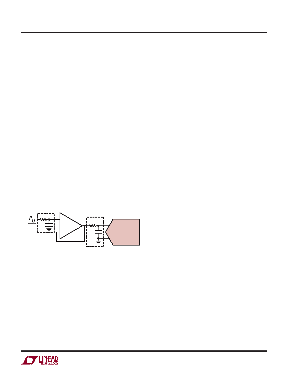
Figure 4. Input Signal Chain
Another filter network consisting of LPF2 should be used
between the buffer and ADC input to both minimize the
noisecontributionofthebufferandtohelpminimizedistur-
bances reflected into the buffer from sampling transients.
Long RC time constants at the analog inputs will slow
down the settling of the analog inputs. Therefore, LPF2
requires a wider bandwidth than LPF1. A buffer amplifier
with a low noise density must be selected to minimize
degradation of the SNR.
5.1
10nF
66nF
50
LPF2
LPF1
BW = 3.2MHz
BW = 48kHz
LTC2370-16
IN+
IN–
237016 F04
–
+
LT6202
VREF
0V
相关PDF资料 |
PDF描述 |
|---|---|
| EEM25DRYF | CONN EDGECARD 50POS DIP .156 SLD |
| VE-B5V-EY | CONVERTER MOD DC/DC 5.8V 50W |
| ESM10DREN | CONN EDGECARD 20POS .156 EYELET |
| EMM10DREN | CONN EDGECARD 20POS .156 EYELET |
| 0210491097 | CABLE JUMPER 1.25MM .030M 39POS |
相关代理商/技术参数 |
参数描述 |
|---|---|
| DC1813A-B | 功能描述:BOARD SAR ADC LTC2368-16 RoHS:是 类别:编程器,开发系统 >> 评估板 - 模数转换器 (ADC) 系列:QuikEval-II™ 产品培训模块:Obsolescence Mitigation Program 标准包装:1 系列:- ADC 的数量:1 位数:12 采样率(每秒):94.4k 数据接口:USB 输入范围:±VREF/2 在以下条件下的电源(标准):- 工作温度:-40°C ~ 85°C 已用 IC / 零件:MAX11645 已供物品:板,软件 |
| DC1813A-C | 功能描述:BOARD SAR ADC LTC2367-16 RoHS:是 类别:编程器,开发系统 >> 评估板 - 模数转换器 (ADC) 系列:QuikEval-II™ 产品培训模块:Obsolescence Mitigation Program 标准包装:1 系列:- ADC 的数量:1 位数:12 采样率(每秒):94.4k 数据接口:USB 输入范围:±VREF/2 在以下条件下的电源(标准):- 工作温度:-40°C ~ 85°C 已用 IC / 零件:MAX11645 已供物品:板,软件 |
| DC1813A-D | 功能描述:BOARD SAR ADC LTC2364-16 RoHS:是 类别:编程器,开发系统 >> 评估板 - 模数转换器 (ADC) 系列:QuikEval-II™ 产品培训模块:Obsolescence Mitigation Program 标准包装:1 系列:- ADC 的数量:1 位数:12 采样率(每秒):94.4k 数据接口:USB 输入范围:±VREF/2 在以下条件下的电源(标准):- 工作温度:-40°C ~ 85°C 已用 IC / 零件:MAX11645 已供物品:板,软件 |
| DC1813A-E | 功能描述:BOARD SAR ADC LTC2369-18 RoHS:是 类别:编程器,开发系统 >> 评估板 - 模数转换器 (ADC) 系列:QuikEval-II™ 产品培训模块:Obsolescence Mitigation Program 标准包装:1 系列:- ADC 的数量:1 位数:12 采样率(每秒):94.4k 数据接口:USB 输入范围:±VREF/2 在以下条件下的电源(标准):- 工作温度:-40°C ~ 85°C 已用 IC / 零件:MAX11645 已供物品:板,软件 |
| DC1813A-F | 功能描述:BOARD SAR ADC LTC2368-18 RoHS:是 类别:编程器,开发系统 >> 评估板 - 模数转换器 (ADC) 系列:QuikEval-II™ 产品培训模块:Obsolescence Mitigation Program 标准包装:1 系列:- ADC 的数量:1 位数:12 采样率(每秒):94.4k 数据接口:USB 输入范围:±VREF/2 在以下条件下的电源(标准):- 工作温度:-40°C ~ 85°C 已用 IC / 零件:MAX11645 已供物品:板,软件 |
发布紧急采购,3分钟左右您将得到回复。