- 您现在的位置:买卖IC网 > PDF目录17028 > DC1813A-A (Linear Technology)BOARD SAR ADC LTC2370-16 PDF资料下载
参数资料
| 型号: | DC1813A-A |
| 厂商: | Linear Technology |
| 文件页数: | 6/24页 |
| 文件大小: | 0K |
| 描述: | BOARD SAR ADC LTC2370-16 |
| 软件下载: | QuikEval II System |
| 设计资源: | DC1813A Design File DC1813A Schematic |
| 标准包装: | 1 |
| 系列: | QuikEval-II™ |
| ADC 的数量: | 1 |
| 位数: | 16 |
| 采样率(每秒): | 2M |
| 数据接口: | 串行,SPI? |
| 输入范围: | 0 ~ VREF |
| 在以下条件下的电源(标准): | 19mW @ 2MSPS |
| 工作温度: | 0°C ~ 70°C |
| 已用 IC / 零件: | LTC2370-16 |
| 已供物品: | 板 |
| 相关产品: | LT6202HS5#TRPBF-ND - IC OP AMP RRIO 100MHZ TSOT23-5 LT6202HS5#TRMPBF-ND - IC OP AMP RRIO 100MHZ TSOT23-5 LTC2370IMS-16#PBF-ND - IC ADC 16BIT SRL/SPI 2M 16-MSOP LTC2370CMS-16#PBF-ND - IC ADC 16BIT SRL/SPI 2M 16-MSOP LTC2370IMS-16#TRPBF-ND - IC ADC 16BIT SRL/SPI 2M 16-MSOP LTC2370IDE-16#TRPBF-ND - IC ADC 16BIT SRL/SPI 2M 16-DFN LTC2370IDE-16#PBF-ND - IC ADC 16BIT SRL/SPI 2M 16-DFN LTC2370HMS-16#TRPBF-ND - IC ADC 16BIT SRL/SPI 2M 16-MSOP LTC2370HMS-16#PBF-ND - IC ADC 16BIT SRL/SPI 2M 16-MSOP LTC2370CMS-16#TRPBF-ND - IC ADC 16BIT SRL/SPI 2M 16-MSOP 更多... |
LTC2370-16
14
237016fa
APPLICATIONS INFORMATION
Power Supply Sequencing
The LTC2370-16 does not have any specific power supply
sequencing requirements. Care should be taken to adhere
to the maximum voltage relationships described in the
Absolute Maximum Ratings section. The LTC2370-16
has a power-on-reset (POR) circuit that will reset the
LTC2370-16 at initial power-up or whenever the power
supply voltage drops below 1V. Once the supply voltage
re-enters the nominal supply voltage range, the POR will
reinitialize the ADC. No conversions should be initiated
until 20s after a POR event to ensure the reinitialization
period has ended. Any conversions initiated before this
time will produce invalid results.
TIMING AND CONTROL
CNV Timing
The LTC2370-16 conversion is controlled by CNV. A ris-
ing edge on CNV will start a conversion and power up the
LTC2370-16.Onceaconversionhasbeeninitiated,itcannot
berestarteduntiltheconversioniscomplete.Foroptimum
performance, CNV should be driven by a clean low jitter
signal. Converter status is indicated by the BUSY output
which remains high while the conversion is in progress.
To ensure that no errors occur in the digitized results, any
additional transitions on CNV should occur within 40ns
from the start of the conversion or after the conversion
has been completed. Once the conversion has completed,
the LTC2370-16 powers down and begins acquiring the
input signal.
Internal Conversion Clock
The LTC2370-16 has an internal clock that is trimmed to
achieveamaximumconversiontimeof322ns.Withamin-
imum acquisition time of 165ns, throughput performance
of 2Msps is guaranteed without any external adjustments.
Auto Power-Down
The LTC2370-16 automatically powers down after a
conversion has been completed and powers up once a
new conversion is initiated on the rising edge of CNV.
During power down, data from the last conversion can
be clocked out. To minimize power dissipation during
power down, disable SDO and turn off SCK. The auto
power-down feature will reduce the power dissipation of
the LTC2370-16 as the sampling frequency is reduced.
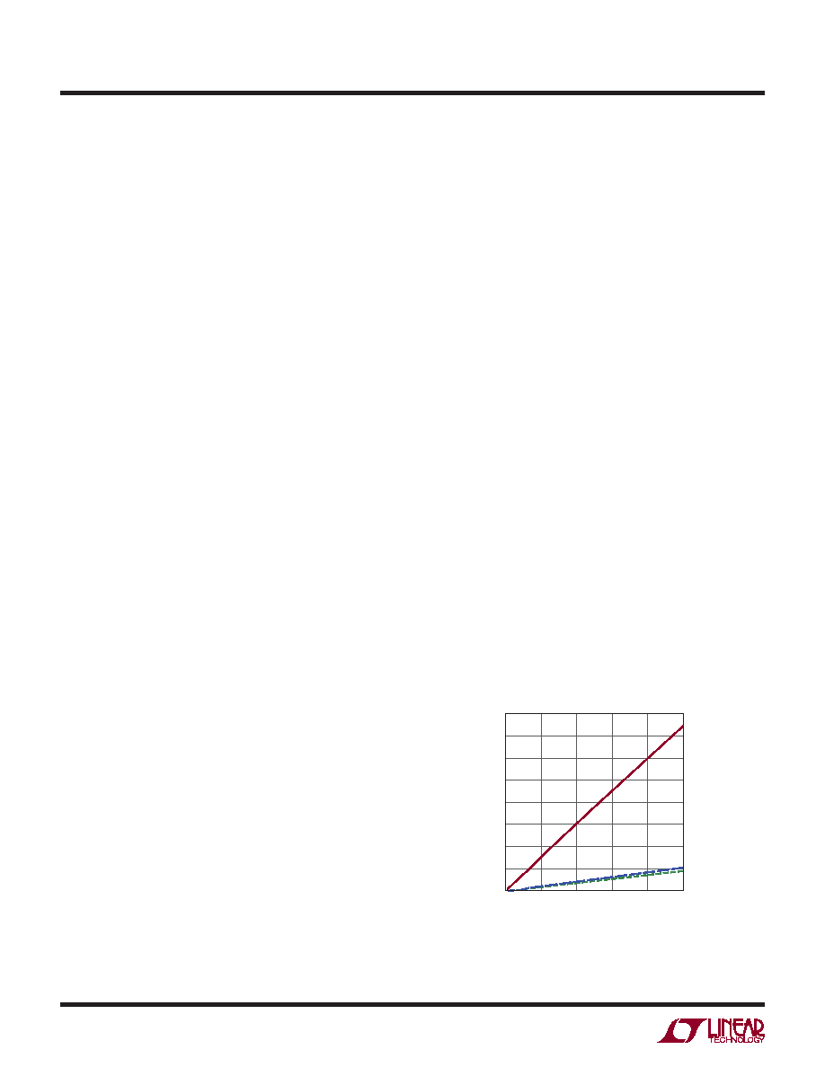
Since power is consumed only during a conversion, the
LTC2370-16remainspowereddownforalargerfractionof
the conversion cycle (tCYC) at lower sample rates, thereby
reducing the average power dissipation which scales with
the sampling rate as shown in Figure 9.
DIGITAL INTERFACE
The LTC2370-16 has a serial digital interface. The flexible
OVDD supply allows the LTC2370-16 to communicate with
any digital logic operating between 1.8V and 5V, including
2.5V and 3.3V systems.
The serial output data is clocked out on the SDO pin when
anexternalclockisappliedtotheSCKpinifSDOisenabled.
Clocking out the data after the conversion will yield the
best performance. With a shift clock frequency of at least
100MHz, a 2Msps throughput is still achieved. The serial
output data changes state on the rising edge of SCK and
can be captured on the falling edge or next rising edge of
SCK. D15 remains valid till the first rising edge of SCK.
The serial interface on the LTC2370-16 is simple and
straightforwardtouse.Thefollowingsectionsdescribethe
operation of the LTC2370-16. Several modes are provided
depending on whether a single or multiple ADCs share the
SPI bus or are daisy chained.
Figure 9. Power Supply Current of the LTC2370-16
Versus Sampling Rate
SAMPLING RATE (kHz)
0
POWER
SUPPLY
CURRENT
(mA)
4
6
2000
1600
237016 F09
2
0
400
800
1200
8
3
5
1
7
IVDD
IREF
IOVDD
相关PDF资料 |
PDF描述 |
|---|---|
| EEM25DRYF | CONN EDGECARD 50POS DIP .156 SLD |
| VE-B5V-EY | CONVERTER MOD DC/DC 5.8V 50W |
| ESM10DREN | CONN EDGECARD 20POS .156 EYELET |
| EMM10DREN | CONN EDGECARD 20POS .156 EYELET |
| 0210491097 | CABLE JUMPER 1.25MM .030M 39POS |
相关代理商/技术参数 |
参数描述 |
|---|---|
| DC1813A-B | 功能描述:BOARD SAR ADC LTC2368-16 RoHS:是 类别:编程器,开发系统 >> 评估板 - 模数转换器 (ADC) 系列:QuikEval-II™ 产品培训模块:Obsolescence Mitigation Program 标准包装:1 系列:- ADC 的数量:1 位数:12 采样率(每秒):94.4k 数据接口:USB 输入范围:±VREF/2 在以下条件下的电源(标准):- 工作温度:-40°C ~ 85°C 已用 IC / 零件:MAX11645 已供物品:板,软件 |
| DC1813A-C | 功能描述:BOARD SAR ADC LTC2367-16 RoHS:是 类别:编程器,开发系统 >> 评估板 - 模数转换器 (ADC) 系列:QuikEval-II™ 产品培训模块:Obsolescence Mitigation Program 标准包装:1 系列:- ADC 的数量:1 位数:12 采样率(每秒):94.4k 数据接口:USB 输入范围:±VREF/2 在以下条件下的电源(标准):- 工作温度:-40°C ~ 85°C 已用 IC / 零件:MAX11645 已供物品:板,软件 |
| DC1813A-D | 功能描述:BOARD SAR ADC LTC2364-16 RoHS:是 类别:编程器,开发系统 >> 评估板 - 模数转换器 (ADC) 系列:QuikEval-II™ 产品培训模块:Obsolescence Mitigation Program 标准包装:1 系列:- ADC 的数量:1 位数:12 采样率(每秒):94.4k 数据接口:USB 输入范围:±VREF/2 在以下条件下的电源(标准):- 工作温度:-40°C ~ 85°C 已用 IC / 零件:MAX11645 已供物品:板,软件 |
| DC1813A-E | 功能描述:BOARD SAR ADC LTC2369-18 RoHS:是 类别:编程器,开发系统 >> 评估板 - 模数转换器 (ADC) 系列:QuikEval-II™ 产品培训模块:Obsolescence Mitigation Program 标准包装:1 系列:- ADC 的数量:1 位数:12 采样率(每秒):94.4k 数据接口:USB 输入范围:±VREF/2 在以下条件下的电源(标准):- 工作温度:-40°C ~ 85°C 已用 IC / 零件:MAX11645 已供物品:板,软件 |
| DC1813A-F | 功能描述:BOARD SAR ADC LTC2368-18 RoHS:是 类别:编程器,开发系统 >> 评估板 - 模数转换器 (ADC) 系列:QuikEval-II™ 产品培训模块:Obsolescence Mitigation Program 标准包装:1 系列:- ADC 的数量:1 位数:12 采样率(每秒):94.4k 数据接口:USB 输入范围:±VREF/2 在以下条件下的电源(标准):- 工作温度:-40°C ~ 85°C 已用 IC / 零件:MAX11645 已供物品:板,软件 |
发布紧急采购,3分钟左右您将得到回复。