- 您现在的位置:买卖IC网 > PDF目录17063 > DC575A (Linear Technology)BOARD DELTA SIGMA ADC LTC2410 PDF资料下载
参数资料
| 型号: | DC575A |
| 厂商: | Linear Technology |
| 文件页数: | 15/48页 |
| 文件大小: | 0K |
| 描述: | BOARD DELTA SIGMA ADC LTC2410 |
| 软件下载: | QuikEval System |
| 设计资源: | DC575A Design File DC575A Schematic |
| 标准包装: | 1 |
| 系列: | QuikEval™ |
| ADC 的数量: | 2 |
| 位数: | 24 |
| 采样率(每秒): | 7.5 |
| 数据接口: | MICROWIRE?,串行,SPI? |
| 工作温度: | 0°C ~ 70°C |
| 已用 IC / 零件: | LTC2410 |
| 已供物品: | 板 |
| 相关产品: | DC590B-ND - BOARD DEMO USB SERIAL CONTROLLER LTC2410IGN#PBF-ND - IC ADC 24BIT DIFF INP/REF 16SSOP LTC2410CGN#TRPBF-ND - IC ADC 24BIT DIFF INP/REF 16SSOP LTC2410IGN#TRPBF-ND - IC ADC 24BIT DIFF INP/REF 16SSOP LTC2410CGN#PBF-ND - IC ADC 24BIT DIFF INP/REF 16SSOP LTC2410CGN#TR-ND - IC ADC 24BIT DIFF INP/REF 16SSOP LTC2410IGN#TR-ND - IC ADC 24BIT DIFF INP/REF 16SSOP LTC2410IGN-ND - IC A/D CONV 24BIT MICRPWR 16SSOP LTC2410CGN-ND - IC ADC 24BIT DIFF INP/REF 16SSOP |
第1页第2页第3页第4页第5页第6页第7页第8页第9页第10页第11页第12页第13页第14页当前第15页第16页第17页第18页第19页第20页第21页第22页第23页第24页第25页第26页第27页第28页第29页第30页第31页第32页第33页第34页第35页第36页第37页第38页第39页第40页第41页第42页第43页第44页第45页第46页第47页第48页
LTC2410
22
APPLICATIO S I FOR ATIO
WU
U
Internal Serial Clock, Autostart Conversion
This timing mode is identical to the internal serial clock,
2-wire I/O described above with one additional feature.
Instead of grounding CS, an external timing capacitor is
tied to CS.
While the conversion is in progress, the CS pin is held
HIGH by an internal weak pull-up. Once the conversion is
complete, the device enters the low power sleep state and
an internal 25nA current source begins discharging the
capacitor tied to CS, see Figure 11. The time the converter
spends in the sleep state is determined by the value of the
external timing capacitor, see Figures 12 and 13. Once the
voltage at CS falls below an internal threshold (
≈1.4V), the
device automatically begins outputting data. The data
output cycle begins on the first rising edge of SCK and
ends on the 32nd rising edge. Data is shifted out the SDO
pin on each falling edge of SCK. The internally generated
serial clock is output to the SCK pin. This signal may be
used to shift the conversion result into external circuitry.
After the 32nd rising edge, CS is pulled HIGH and a new
conversion is immediately started. This is useful in appli-
cations requiring periodic monitoring and ultralow power.
Figure 14 shows the average supply current as a function
of capacitance on CS.
It should be noticed that the external capacitor discharge
current is kept very small in order to decrease the con-
verter power dissipation in the sleep state. In the autostart
mode, the analog voltage on the CS pin cannot be ob-
served without disturbing the converter operation using a
regular oscilloscope probe. When using this configura-
tion, it is important to minimize the external leakage
current at the CS pin by using a low leakage external
capacitor and properly cleaning the PCB surface.
The internal serial clock mode is selected every time the
voltage on the CS pin crosses an internal threshold volt-
age. An internal weak pull-up at the SCK pin is active while
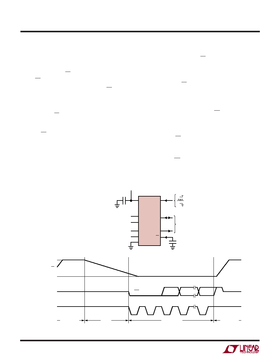
Figure 11. Internal Serial Clock, Autostart Operation
SDO
Hi-Z
SCK
(INTERNAL)
CS
VCC
GND
2410 F11
BIT 0
SIG
BIT 29
BIT 30
SLEEP
DATA OUTPUT
CONVERSION
EOC
BIT 31
= 50Hz REJECTION
= EXTERNAL OSCILLATOR
= 60Hz REJECTION
VCC
VCC
FO
REF+
REF–
SCK
IN+
IN –
SDO
GND
CS
214
3
4
13
5
6
12
1, 7, 8, 9, 10, 15, 16
11
REFERENCE
VOLTAGE
0.1V TO VCC
ANALOG INPUT RANGE
–0.5VREF TO 0.5VREF
2-WIRE
INTERFACE
1
F
2.7V TO 5.5V
LTC2410
CEXT
相关PDF资料 |
PDF描述 |
|---|---|
| MIC2004-1.2YML TR | IC DISTRIBUTION SW 1.2A 6-MLF |
| AD9779A-DPG2-EBZ | BOARD EVALUATION FOR AD9779A |
| DC955A | BOARD DELTA SIGMA ADC LTC2483 |
| SDR0604-181KL | INDUCTOR POWER 180UH 0.38A SMD |
| AP2186SG-13 | IC USB PWR SWITCH 1.5A DUAL 8SOP |
相关代理商/技术参数 |
参数描述 |
|---|---|
| DC579A | 功能描述:BOARD DAC LTC2600 RoHS:是 类别:编程器,开发系统 >> 评估板 - 数模转换器 (DAC) 系列:QuikEval™ 产品培训模块:Lead (SnPb) Finish for COTS Obsolescence Mitigation Program 标准包装:1 系列:- DAC 的数量:4 位数:12 采样率(每秒):- 数据接口:串行,SPI? 设置时间:3µs DAC 型:电流/电压 工作温度:-40°C ~ 85°C 已供物品:板 已用 IC / 零件:MAX5581 |
| DC579A | 制造商:Linear Technology 功能描述:LTC2600 EVALUATION KIT |
| DC57F10W06P6 | 制造商:Conesys 功能描述:CONN 26482 CIRC PIN 6 POS CRMP ST CBL MNT - Bulk |
| DC57F10W06P6-CO | 制造商:Conesys 功能描述:CONN 26482 CIRC PIN 6 POS CRMP ST CBL MNT - Bulk |
| DC57F10W06PN | 制造商:Conesys 功能描述:CONN 26482 CIRC PIN 6 POS CRMP ST CBL MNT - Bulk |
发布紧急采购,3分钟左右您将得到回复。