- 您现在的位置:买卖IC网 > PDF目录17063 > DC575A (Linear Technology)BOARD DELTA SIGMA ADC LTC2410 PDF资料下载
参数资料
| 型号: | DC575A |
| 厂商: | Linear Technology |
| 文件页数: | 20/48页 |
| 文件大小: | 0K |
| 描述: | BOARD DELTA SIGMA ADC LTC2410 |
| 软件下载: | QuikEval System |
| 设计资源: | DC575A Design File DC575A Schematic |
| 标准包装: | 1 |
| 系列: | QuikEval™ |
| ADC 的数量: | 2 |
| 位数: | 24 |
| 采样率(每秒): | 7.5 |
| 数据接口: | MICROWIRE?,串行,SPI? |
| 工作温度: | 0°C ~ 70°C |
| 已用 IC / 零件: | LTC2410 |
| 已供物品: | 板 |
| 相关产品: | DC590B-ND - BOARD DEMO USB SERIAL CONTROLLER LTC2410IGN#PBF-ND - IC ADC 24BIT DIFF INP/REF 16SSOP LTC2410CGN#TRPBF-ND - IC ADC 24BIT DIFF INP/REF 16SSOP LTC2410IGN#TRPBF-ND - IC ADC 24BIT DIFF INP/REF 16SSOP LTC2410CGN#PBF-ND - IC ADC 24BIT DIFF INP/REF 16SSOP LTC2410CGN#TR-ND - IC ADC 24BIT DIFF INP/REF 16SSOP LTC2410IGN#TR-ND - IC ADC 24BIT DIFF INP/REF 16SSOP LTC2410IGN-ND - IC A/D CONV 24BIT MICRPWR 16SSOP LTC2410CGN-ND - IC ADC 24BIT DIFF INP/REF 16SSOP |
第1页第2页第3页第4页第5页第6页第7页第8页第9页第10页第11页第12页第13页第14页第15页第16页第17页第18页第19页当前第20页第21页第22页第23页第24页第25页第26页第27页第28页第29页第30页第31页第32页第33页第34页第35页第36页第37页第38页第39页第40页第41页第42页第43页第44页第45页第46页第47页第48页
LTC2410
27
APPLICATIO S I FOR ATIO
WU
U
In addition to the input sampling charge, the input ESD
protection diodes have a temperature dependent leakage
current. This current, nominally 1nA (
±10nA max), results
in a small offset shift. A 100
source resistance will create
a 0.1
V typical and 1V maximum offset voltage.
Reference Current
In a similar fashion, the LTC2410 samples the differential
reference pins REF+ and REF– transfering small amount of
charge to and from the external driving circuits thus
producing a dynamic reference current. This current does
not change the converter offset, but it may degrade the
gain and INL performance. The effect of this current can be
analyzed in the same two distinct situations.
For relatively small values of the external reference capaci-
tors (CREF < 0.01F), the voltage on the sampling capacitor
settles almost completely and relatively large values for
the source impedance result in only small errors. Such
values for CREF will deteriorate the converter offset and
gain performance without significant benefits of reference
filtering and the user is advised to avoid them.
Larger values of reference capacitors (CREF > 0.01F) may
be required as reference filters in certain configurations.
Such capacitors will average the reference sampling charge
and the external source resistance will see a quasi con-
stant reference differential impedance. When FO = LOW
(internal oscillator and 60Hz notch), the typical differential
reference resistance is 1.3M
which will generate a gain
error of approximately 0.38ppm for each ohm of source
resistance driving REF+ or REF–. When FO = HIGH (internal
oscillator and 50Hz notch), the typical differential refer-
ence resistance is 1.56M
whichwillgenerateagainerror
of approximately 0.32ppm for each ohm of source resis-
tance driving REF+ or REF–. When FO is driven by an
external oscillator with a frequency fEOSC (external conver-
sion clock operation), the typical differential reference
resistance is 0.20 1012/fEOSC and each ohm of source
resistance drving REF+ or REF– will result in
2.47 10–6 fEOSCppm gain error. The effect of the source
resistance on the two reference pins is additive with
respect to this gain error. The typical +FS and –FS errors
for various combinations of source resistance seen by the
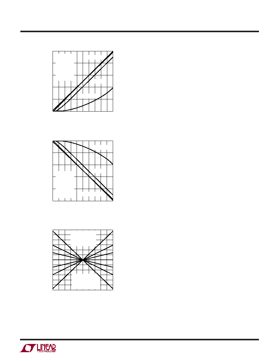
Figure 19. +FS Error vs RSOURCE at IN
+ or IN– (Large CIN)
Figure 20. –FS Error vs RSOURCE at IN+ or IN– (Large CIN)
Figure 21. Offset Error vs Common Mode Voltage
(VINCM = IN+ = IN–) and Input Source Resistance Imbalance
(
RIN = RSOURCEIN+ – RSOURCEIN–) for Large CIN Values (CIN ≥ 1F)
RSOURCE ()
0 100 200 300 400 500 600 700 800 900 1000
+FS
ERROR
(ppm
OF
V
REF
)
2410 F19
300
240
180
120
60
0
VCC = 5V
REF+ = 5V
REF – = GND
IN+ = 3.75V
IN– = 1.25V
FO = GND
TA = 25°C
CIN = 0.01F
CIN = 0.1F
CIN = 1F, 10F
RSOURCE ()
0 100 200 300 400 500 600 700 800 900 1000
–
FS
ERROR
(ppm
OF
V
REF
)
2410 F20
0
–60
–120
–180
–240
–300
VCC = 5V
REF+ = 5V
REF – = GND
IN+ = 1.25V
IN– = 3.75V
FO = GND
TA = 25°C
CIN = 0.01F
CIN = 0.1F
CIN = 1F, 10F
VINCM (V)
0
0.5
1
1.5
2
2.5
3
3.5
4
4.5
5
OFFSET
ERROR
(ppm
OF
V
REF
)
2410 F21
120
100
80
60
40
20
0
–20
–40
–60
–80
–100
–120
FO = GND
TA = 25°C
RSOURCEIN– = 500
CIN = 10F
VCC = 5V
REF+ = 5V
REF – = GND
IN+ = IN– = VINCM
A:
RIN = +400
B:
RIN = +200
C:
RIN = +100
D:
RIN = 0
E:
RIN = –100
F:
RIN = –200
G:
RIN = –400
A
B
C
D
E
F
G
相关PDF资料 |
PDF描述 |
|---|---|
| MIC2004-1.2YML TR | IC DISTRIBUTION SW 1.2A 6-MLF |
| AD9779A-DPG2-EBZ | BOARD EVALUATION FOR AD9779A |
| DC955A | BOARD DELTA SIGMA ADC LTC2483 |
| SDR0604-181KL | INDUCTOR POWER 180UH 0.38A SMD |
| AP2186SG-13 | IC USB PWR SWITCH 1.5A DUAL 8SOP |
相关代理商/技术参数 |
参数描述 |
|---|---|
| DC579A | 功能描述:BOARD DAC LTC2600 RoHS:是 类别:编程器,开发系统 >> 评估板 - 数模转换器 (DAC) 系列:QuikEval™ 产品培训模块:Lead (SnPb) Finish for COTS Obsolescence Mitigation Program 标准包装:1 系列:- DAC 的数量:4 位数:12 采样率(每秒):- 数据接口:串行,SPI? 设置时间:3µs DAC 型:电流/电压 工作温度:-40°C ~ 85°C 已供物品:板 已用 IC / 零件:MAX5581 |
| DC579A | 制造商:Linear Technology 功能描述:LTC2600 EVALUATION KIT |
| DC57F10W06P6 | 制造商:Conesys 功能描述:CONN 26482 CIRC PIN 6 POS CRMP ST CBL MNT - Bulk |
| DC57F10W06P6-CO | 制造商:Conesys 功能描述:CONN 26482 CIRC PIN 6 POS CRMP ST CBL MNT - Bulk |
| DC57F10W06PN | 制造商:Conesys 功能描述:CONN 26482 CIRC PIN 6 POS CRMP ST CBL MNT - Bulk |
发布紧急采购,3分钟左右您将得到回复。